
Eureka
For R&D, Eureka makes reading and utilizing patents & technical documents easy.
Eureka AIR
Designed for self-driven R&D workflows. Generate viable solutions, solve complex R&D challenges, empower your innovation with AI.

Eureka Materials
Designed for material experts only. Revolutionize your material R&D, from search, analyze, to developing new materials.

TechResearch
Generate reliable direction feasibility study reports for your R&D in just a few steps.

TechSeek
Discover and master advanced knowledge NOW. Basics, ideas, possibilities, all at once.

TechMind
As an expert in R&D Theories, TechMind can generates customized viable solutions instantly.

TechRisk
Analyze your overall solution with one click, know your potential R&D risks in advance.

TechMonitor
Get weekly tech updates, stay abreast of the latest tech innovations and key insights.
Surface treating agent and method for p-type bismuth telluride-based material applied to thermoelectric device
A technology of surface treatment agent and bismuth telluride base crystal, which is applied in the manufacture/treatment of thermoelectric devices, thermoelectric device node lead-out materials, chemical instruments and methods, etc., can solve the problem of increasing production links and production costs, p-type tellurium Bismuth-based wafer damage, reduced yield and production efficiency and other issues, to achieve the effect of improving yield and production efficiency, improving interface bonding strength, reducing interface contact resistance and interface thermal resistance
- Summary
- Abstract
- Description
- Claims
- Application Information
AI Technical Summary
Problems solved by technology
Method used
Image

Examples
Embodiment 1
[0035] A surface treatment method for a p-type bismuth telluride-based material, comprising the following steps:
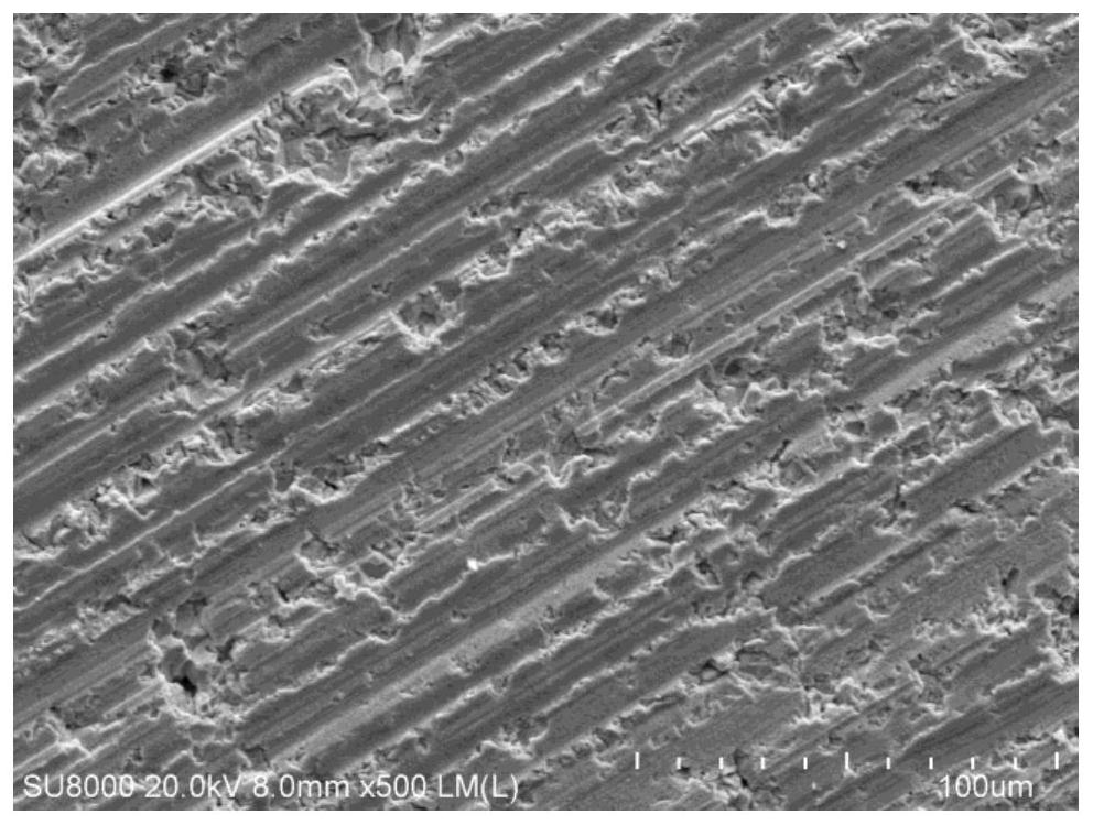
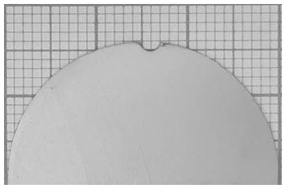
[0036] 1) A semicircular p-type bismuth telluride-based wafer with a diameter of 30 mm and a thickness of 0.3 mm is washed with acetone and degreased to remove surface pollutants, dehydrated with absolute ethanol, and dried with an OLS5000 laser scanning microscope for surface roughness testing. The surface is rough The degree Sa is 0.197 μm, then immersed in the roughening solution (the composition of the roughening solution is 10% (volume) of hydrochloric acid, 40% (volume) of hydrogen peroxide, 5% (volume) of nitric acid, and the balance is water), and the roughening temperature is 30 ℃, coarsening time 5min;
[0037] 2) The roughened p-type bismuth telluride-based wafer in step 1) is transferred to ash removal solution (the composition of the ash removal solution is 50% (volume) of hydrofluoric acid, 10% (volume) of hydrochloric acid, and 5% (volume) of nitric...
Embodiment 2
[0059] A surface treatment method for a p-type bismuth telluride-based material, comprising the following steps:
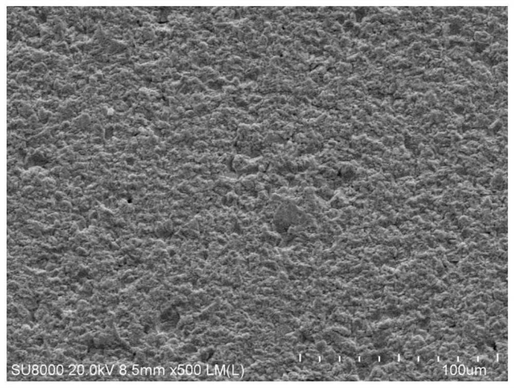
[0060] 1) A semicircular p-type bismuth telluride-based wafer with a diameter of 30 mm and a thickness of 0.3 mm was washed with acetone and degreased to remove surface pollutants, dehydrated with absolute ethanol, dried, and then observed by SEM, and then immersed in a roughening solution (roughened The composition of the chemical solution is 20% (volume) of hydrochloric acid, 30% (volume) of hydrogen peroxide, 5% (volume) of nitric acid, and the balance is water), the roughening temperature is 30 ° C, and the roughening time is 10 minutes;
[0061] 2) The roughened p-type bismuth telluride-based wafer in step 1) is transferred to ash removal solution (the composition of the ash removal solution is 40% (volume) of hydrofluoric acid, 10% (volume) of hydrochloric acid, and 5% (volume) of nitric acid ( volume), the balance is water), and the ash removal temperature ...
PUM
| Property | Measurement | Unit |
|---|---|---|
| Diameter | aaaaa | aaaaa |
| Thickness | aaaaa | aaaaa |
| Roughness | aaaaa | aaaaa |
Abstract
Description
Claims
Application Information
 - R&D Engineer
- R&D Manager
- IP Professional
- Industry Leading Data Capabilities
- Powerful AI technology
- Patent DNA Extraction
Browse by: Latest US Patents, China's latest patents, Technical Efficacy Thesaurus, Application Domain, Technology Topic, Popular Technical Reports.
© 2024 PatSnap. All rights reserved.Legal|Privacy policy|Modern Slavery Act Transparency Statement|Sitemap|About US| Contact US: help@patsnap.com