High-speed mini photoelectric conversion module design and process method

A technology of photoelectric conversion module and process method, applied in the direction of light guide, optics, optical components, etc., can solve the problems of high manufacturing process difficulty, low yield, supply chain limitation, etc., to reduce the plate making process difficulty, low cost, and improve the The effect of yield

Inactive Publication Date: 2021-03-16
JIANGSU ALLRAY
View PDF8 Cites 0 Cited by
  • Summary
  • Abstract
  • Description
  • Claims
  • Application Information

AI Technical Summary

Problems solved by technology

[0004] The purpose of the present invention is to provide a high-speed mini photoelectric conversion module design and process method to solve the traditional high-speed mini photoelectric conversion module proposed in the above background technology. The upper board of the PCB adopts a 10-layer hard board, and the lower board adopts a 6-layer soft board. The design of the design, the electrical connection between the upper board and the lower board is directly realized by the 6-layer soft board. When the shell is assembled, the 6-layer soft board needs to be bent. In order to meet the requirements of the shell assembly space, the thickness of the 6-layer soft board needs to be It is difficult to control the plate within 0.4mm. Generally, PCB board factories are unable to process, but they have the ability to process board factories. The price is expensive and the yield is not high, so the supply chain is greatly restricted. In addition, in order to achieve optical coupling needs In order to meet the mechanical strength and heat dissipation requirements, it is necessary to add a metal patching process to the 6-layer flexible board. The so-called metal patching process is to precisely adhere the pre-designed metal patching board to the PCB soft board through adhesive hot pressing. In this way, the mechanical strength of the PCB soft board can be increased, and at the same time, it can assist the heat equalization and heat dissipation of the heating device. This process is a precision process, and the general PCB board factory cannot complete it. The metal wall patch is composed of a substrate, a large boss, and a small boss. , the thickness of the substrate is 0.35mm, the thickness of the large boss is 0.35mm, and the thickness of the small boss is 0.15mm. Among them, the flatness of the substrate surface is not less than 0.1mm, the flatness of the large boss is not less than 0.05mm, and the flatness of the small boss is not less than 0.01mm, the parallelism of the substrate surface is not less than 0.05mm, the connection between the substrate, the large boss, and the small boss is cleaned around, and the chamfer is less than 0.1mm. The manufacturing process is difficult and exceeds the general machining accuracy, subject to the PCB plate making process Complicated, difficult processing of metal patching boards, high adhesion precision requirements, etc., this type of photoelectric conversion module is difficult to mass-produce and the yield is very low

Method used


Image

  • High-speed mini photoelectric conversion module design and process method
  • High-speed mini photoelectric conversion module design and process method
  • High-speed mini photoelectric conversion module design and process method

Examples


Embodiment 1

[0023] The processing method of the present embodiment comprises the following steps:

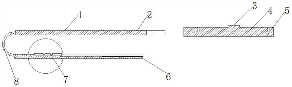
[0024] S1. First, the PCB part adopts an integrated design scheme of 8-layer hard board plus 4-layer soft board plus 6-layer hard board. By reducing the number of soft board layers, the thickness of the soft board is successfully controlled within 0.35mm, which reduces the difficulty of PCB plate making process , Improve the yield of PCB plate making, increase the reliability of the long-term bending of the flexible board, replace the metal wall patch with the design of tungsten copper heat sink and ceramic gasket, the process is simple, and the cost is low.

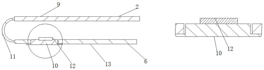
[0025] S2. Then, at the transmitting end, 12 differential electrical signals are input to the 12-channel VCSEL driver through the 12-channel data port of the optical module, and the 12-channel VCSEL driver simultaneously modulates and drives the 12-channel VCSEL to emit light, and the 12-channel lens array couples the 12-channel optica...

Embodiment 2

[0032] The difference from Embodiment 1 is that:

[0033] The processing method of the present embodiment comprises the following steps:

[0034] S1. First, the PCB part is designed with 10-layer hard board and 6-layer soft board. The thickness of the 6-layer soft board is controlled at 0.4mm. The manufacturing process is very difficult, and the yield is not high. Paste the metal wall board on the 6-layer soft board. The upper process is complicated and difficult, and the yield rate is not high.

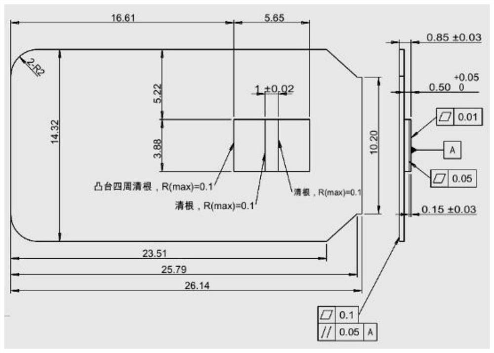
[0035] S2. Then, the design drawing of the metal wall patching board requires that the surface flatness of the metal wall patching board substrate is not less than 0.1mm, the surface flatness of the large boss is not less than 0.05mm, and the surface roughness of the small boss is not less than 0.01mm. The joints of the platform and the small boss are cleaned around, and the chamfer is less than 0.1mm. The manufacturing process is difficult and exceeds the general machining accuracy...


PUM

PropertyMeasurementUnit
thicknessaaaaaaaaaa

Abstract

The invention discloses a high-speed mini photoelectric conversion module design and process method. The process method comprises the following steps: S1, firstly employing an integrated design schemeof eight hard boards, four soft boards and six hard boards for a PCB part, successfully controlling the thickness of the soft boards to be within 0.35 mm through reducing the number of layers of thesoft boards in order to reduce the difficulty of a PCB plate making process, improve the rate of finished products of PCB plate making and improve the reliability of long-term bending of the soft plate part, and replacing the metal wall-filling plate by the design of the tungsten-copper heat sink and the ceramic gasket to make the process simple and the cost low; and S2, inputting 12 paths of differential electric signals to a 12-channel VCSEL drive through 12 paths of data ports of an optical module at a transmitting end, simultaneously modulating and driving the 12 paths of VCSEL to emit light through the 12-channel VCSEL drive, coupling the 12 paths of optical signals to an optimal state through a 12-channel lens array, and transmitting the 12 paths of optical signals to a far-end signal processor through an optical fiber, thereby realizing electro-optical conversion.

Description

technical field [0001] The invention relates to the technical field of aerospace measurement and control transmission system application and industrial automation control system, specifically a design and process method of a high-speed mini photoelectric conversion module. Background technique [0002] In recent years, the rise of network and business applications such as cloud computing, Internet of Things, and mobile Internet has put forward high bandwidth and bearer requirements for the underlying transport network, especially for network bandwidth, fast service provision, and network flexibility. have raised higher demands. A high-speed mini photoelectric conversion module. The photoelectric conversion module includes 12 channels of transmission and 12 channels of reception. The single channel rate is 10Gbps. The 12 channels of transmission and reception can work at the same time. The maximum transmission rate is 120Gbps. It is a mainstream optical module product in the ...

Claims


Application Information

Patent Timeline
Patent Type & Authority Applications(China)
IPC IPC(8): G02B6/42
CPCG02B6/428G02B6/4296G02B6/4204G02B6/4239G02B6/4256G02B6/4287
Inventor 王波于佩杨丽于凯
Owner JIANGSU ALLRAY
Why Eureka
Try Eureka