Inter-layer bonding sheet for multi-layer board and preparation method and application of inter-layer bonding sheet
A multi-layer board and bonding sheet technology, which is applied in multi-layer circuit manufacturing, coating, printed circuit manufacturing, etc., can solve the problems of poor heat resistance reliability, high dielectric constant, and high peel strength of PTFE multi-layer board bonding , to meet the needs of high frequency signals and stability, low dielectric constant and dielectric loss tangent, good chemical resistance and mechanical properties
- Summary
- Abstract
- Description
- Claims
- Application Information
AI Technical Summary
Problems solved by technology
Method used
Image
Examples
Embodiment 1
[0089] This embodiment provides an interlayer bonding sheet for a multilayer board, the preparation method of which is as follows:
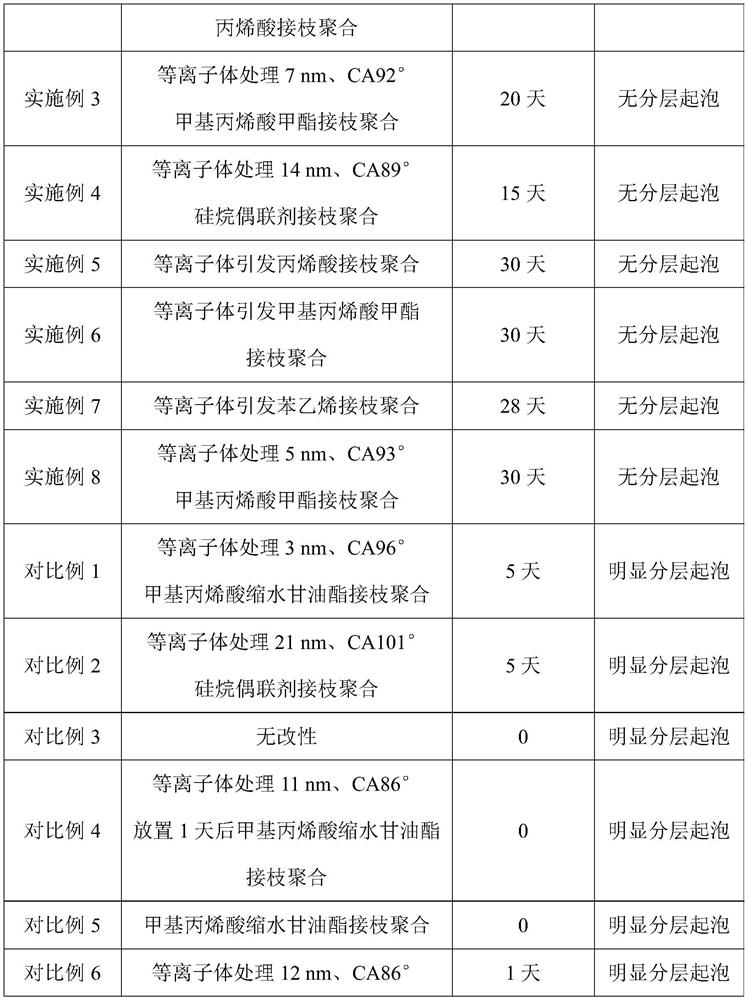
[0090] (1) Preparation of modified PTFE substrate: the PTFE substrate with a thickness of 0.9mm is cleaned and dried with ethanol; then it is placed in a low-temperature plasma generator, and the setting voltage is 3000V, and the vacuum degree of the system is 560Pa. RF power is 3kW, in Ar, H 2 In a mixed atmosphere (Ar, H 2The volume ratio is 9:1) and treated for 240s; placed in the air for 10min, then immersed in glycidyl methacrylate containing 0.002mol / L diethylpropylbenzene peroxide, graft polymerization at 130°C for 40min under nitrogen protection , to obtain a modified PTFE substrate;
[0091] (2) Place the modified PTFE substrate obtained in step (1) for 28 days, then roll-coat dielectric resin treatment solution I on the upper and lower surfaces respectively to obtain a dielectric resin layer with a thickness of 25 μm on the upper and ...
Embodiment 2
[0093] This embodiment provides an interlayer bonding sheet for a multilayer board, the preparation method of which is as follows:
[0094] (1) Preparation of modified PTFE substrate: the PTFE substrate with a thickness of 0.5mm is cleaned and dried with acetone; then it is placed in a low-temperature plasma generator, and the setting voltage is 3000V, and the system vacuum is 155Pa. RF power is 1kW, at N 2 , H 2 In the mixed atmosphere (N 2 , H 2 The volume ratio is 8:2) and treated for 600s; placed in the air for 10min, then immersed in acrylic acid containing 0.004mol / L dibenzoyl peroxide, and grafted and polymerized at 90°C for 140min under the protection of nitrogen to obtain modified PTFE Substrate;
[0095] (2) The modified PTFE substrate obtained in step (1) was placed for 5 days, and then the upper and lower surfaces were roll-coated with dielectric resin treatment solution I to obtain a dielectric resin layer with a thickness of 40 μm on the upper and lower surfa...
Embodiment 3
[0097] This embodiment provides an interlayer bonding sheet for a multilayer board, the preparation method of which is as follows:
[0098] (1) Preparation of modified PTFE substrate: the PTFE substrate with a thickness of 1.3mm is cleaned and dried with ethanol; then it is placed in a low-temperature plasma generator, and the setting voltage is 6000V, and the system vacuum is 1224Pa. RF power is 5kW, treated in Ar atmosphere for 60s; placed in air for 10min, then immersed in methyl methacrylate containing 0.006mol / L dibenzoyl peroxide, grafted and polymerized at 105°C for 70min under nitrogen protection , to obtain a modified PTFE substrate;
[0099] (2) The modified PTFE substrate obtained in step (1) was placed for 20 days, and then the upper and lower surfaces were roll-coated with dielectric resin treatment solution I to obtain a dielectric resin layer with a thickness of 50 μm on the upper and lower surfaces, and cured at 210 ° C for 3 hours. , to obtain the interlayer ...
PUM
| Property | Measurement | Unit |
|---|---|---|
| thickness | aaaaa | aaaaa |
| particle size | aaaaa | aaaaa |
| thickness | aaaaa | aaaaa |
Abstract
Description
Claims
Application Information

