Photothermoelectric detector based on platinum diselenide bismuth telluride and preparation method thereof
A bismuth telluride and photothermoelectric technology, which is used in the manufacture/processing of thermoelectric devices, electrical radiation detectors, and lead wire materials for thermoelectric devices, can solve the problems of difficulty in taking into account broadband and high responsivity. The effect of mild conditions and simple device structure
- Summary
- Abstract
- Description
- Claims
- Application Information
AI Technical Summary
Problems solved by technology
Method used
Image
Examples
Embodiment 1
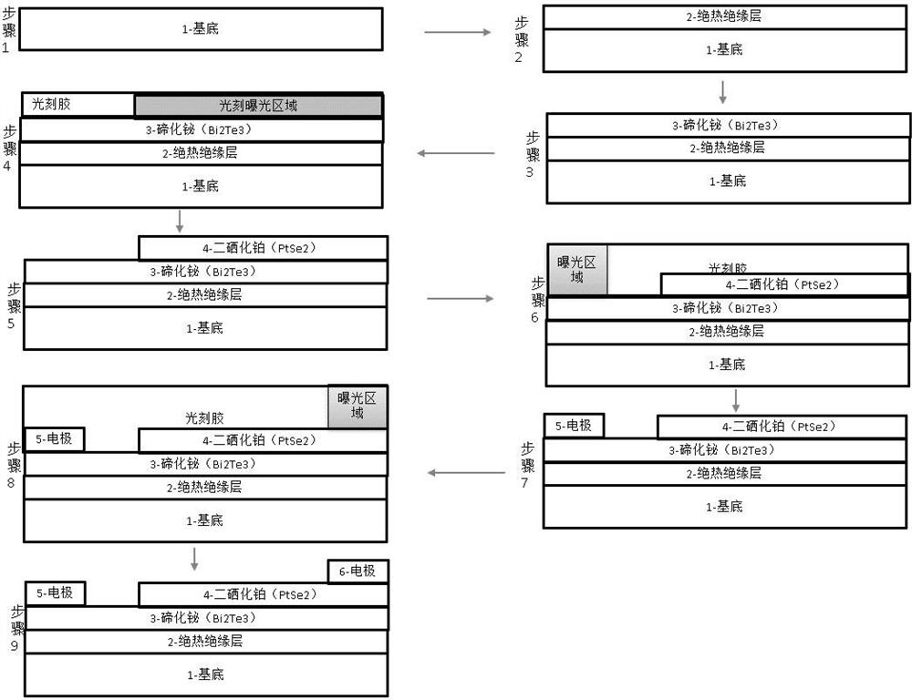
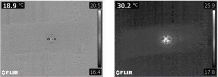
[0050] Such as figure 1 Shown is an implementation case of the photopyroelectric detector based on platinum diselenide bismuth telluride and its preparation method in the present invention. Such as figure 2 As shown, it is prepared by the following method:
[0051] 1) Substrate preparation: Clean the Si substrate with ultrasonic vibrations such as acetone and hydrogen peroxide, and dry it with nitrogen for later use;
[0052] 2) Deposit a layer of thermal insulation layer on the substrate, the optional material is SiO 2 , thickness 200nm;
[0053] 3) Deposition of Bi 2 Te 3Thin film: preheat the clean substrate obtained in the above steps to 350-400 degrees Celsius, and deposit a layer of Bi on the substrate by magnetron sputtering 2 Te 3 , the sputtering parameters are: air pressure, 4.0-4.5Pa, 1 hour room temperature sputtering time, sputtering power 10-20W, sample target thickness: 50 nm; (Note: a mask plate can be preset on the substrate to deposit the cycle Sexua...
Embodiment 2
[0076] Such as figure 1 Shown is an implementation case of the photopyroelectric detector based on platinum diselenide bismuth telluride and its preparation method in the present invention. Such as figure 2 As shown, it is prepared by the following method:
[0077] 1) Substrate preparation: Clean the polyimide substrate with deionized water, absolute ethanol and other ultrasonic vibrations, and dry it with nitrogen for later use;
[0078] 2) Deposit a layer of thermal insulation layer on the substrate, the optional material is SiN, with a thickness of 300nm;
[0079] 3) Deposition of Bi 2 Te 3 Thin film: preheat the clean substrate obtained in the above steps to 350-400 degrees Celsius, and deposit a layer of Bi on the substrate by magnetron sputtering 2 Te 3 , the sputtering parameters are: air pressure, 4.0-4.5Pa, 1 hour room temperature sputtering time, sputtering power 10-20W, sample target thickness: 200 nm; (Note: a mask can be preset on the substrate to deposit t...
PUM
| Property | Measurement | Unit |
|---|---|---|
| Thickness | aaaaa | aaaaa |
| Thickness | aaaaa | aaaaa |
| Thickness | aaaaa | aaaaa |
Abstract
Description
Claims
Application Information


