MEMS thermopile infrared detector and manufacturing method thereof

The technology of an infrared detector and a manufacturing method, which is applied in the field of infrared detection, can solve the problems of low infrared absorption rate, increased measurement error, difficulty in batch preparation, etc., so as to enhance infrared detection performance, reduce measurement error, and controllability. strong effect

Active Publication Date: 2021-05-14
山东新港电子科技有限公司
View PDF19 Cites 0 Cited by
  • Summary
  • Abstract
  • Description
  • Claims
  • Application Information

AI Technical Summary

Problems solved by technology

When subjected to strong electromagnetic radiation, the measurement error increases and the reliability decreases
On the other hand, the absorption efficiency of infrared radiation in the infrared absorption region greatly affects the performance of the detector. However, the infrared absorption region materials of traditional MEMS thermopile infrared detectors are usually silicon nitride and silicon oxide dielectric films. The infrared absorption rate is not high; coating a light-absorbing layer such as carbon black on a dielectric film or preparing a micro-nano structure such as black silicon can improve the infrared absorption rate to a certain extent, but these methods are either incompatible with the current mature CMOS process, or can be Poor controllability and difficult batch preparation

Method used


Image

  • MEMS thermopile infrared detector and manufacturing method thereof
  • MEMS thermopile infrared detector and manufacturing method thereof
  • MEMS thermopile infrared detector and manufacturing method thereof

Examples


Embodiment 1

[0077] Embodiment 1: as Figure 9 As shown, a MEMS thermopile infrared detector, including:

[0078] The substrate 10 is provided with a heat insulating cavity 11;

[0079] a support layer 20 formed on the upper surface of the substrate 10;

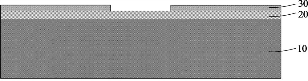
[0080] The thermopile unit is formed on the supporting layer 20, and is partially located above the heat insulation cavity 11, and includes a first thermocouple layer 30, a first insulating layer 40, and a second thermocouple layer 50 from bottom to top, and the first The thermocouple layer 30 and the second thermocouple layer 50 are connected through the first contact hole 41 in the first insulating layer 40 to form a thermopile;

[0081] The second insulating layer 60 covers the second thermocouple layer 50;

[0082] The electromagnetic shielding layer 70 is formed on the upper surface of the second insulating layer 60;

[0083] The infrared absorbing layer 80 covers the electromagnetic shielding layer 70 , and partially etches a se...

Embodiment 2

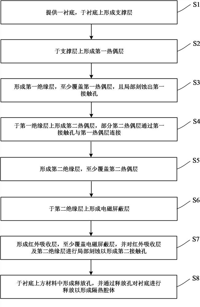
[0092] Embodiment 2: as figure 1 As shown, the manufacturing method of the above-mentioned MEMS thermopile infrared detector comprises the following steps:

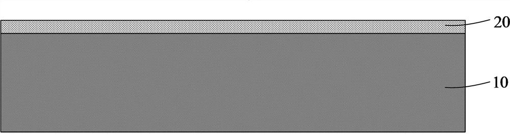
[0093] S1. A substrate 10 is provided, and a support layer 20 is formed on the substrate 10, such as figure 2 shown.

[0094] Specifically, the substrate 10 is a common semiconductor substrate, including but not limited to a silicon substrate, a germanium substrate, an SOI substrate, and a GeOI substrate; in an embodiment of the present invention, the substrate 10 is a single crystal silicon substrate.

[0095] Specifically, the material of the support layer 20 is one or a combination of silicon oxide and silicon nitride, wherein silicon oxide can be formed by thermal oxidation, low pressure chemical vapor deposition, plasma chemical vapor deposition, and silicon nitride It can be formed by low-pressure chemical vapor deposition or plasma chemical vapor deposition; in an embodiment of the present invention, the suppor...


PUM


Abstract

The invention discloses an MEMS thermopile infrared detector and a manufacturing method thereof, and the infrared detector comprises: a substrate, which is provided with a heat insulation cavity; a supporting layer, which is formed on the upper surface of the substrate; a thermopile unit, which is formed on the supporting layer and sequentially comprises a first thermocouple layer, a first insulating layer and a second thermocouple layer from bottom to top, wherein the first thermocouple layer and the second thermocouple layer are connected through a first contact hole in the first insulating layer; a second insulating layer, an electromagnetic shielding layer and an infrared absorption layer, which are sequentially formed on the thermopile unit, wherein the infrared absorption layer and the second insulating layer are partially etched to form a second contact hole. According to the invention, the electromagnetic shielding layer which can be grounded is arranged below the infrared absorption layer, so that electromagnetic shielding is realized, measurement errors are reduced, and the reliability of the detector is improved; in addition, the electromagnetic shielding layer can reflect infrared radiation generated by a detected object, and secondary absorption of the infrared absorption layer is facilitated, so that the infrared absorption rate of the infrared absorption layer is improved, and the infrared detection performance is enhanced.

Description

technical field [0001] The invention belongs to the technical field of infrared detection, in particular to a MEMS thermopile infrared detector and a manufacturing method thereof. Background technique [0002] With the development of Micro-Electro-Mechanical System (MEMS) technology, infrared detectors based on MEMS thermopiles are favored due to their small size, low power consumption, high sensitivity, and non-contact temperature measurement. It is widely used in military and civilian fields, such as military detection, radar guidance, security early warning, spectral analysis, remote temperature measurement, etc. [0003] The MEMS thermopile infrared detector is an uncooled detector based on the Seebeck effect, which mainly includes a thermopile densely packed on a suspended support film and an infrared absorption region located in the center of the thermopile. The infrared absorption region absorbs infrared radiation and converts it into heat, and then generates a tempe...

Claims


Application Information

Patent Timeline
Patent Type & Authority Applications(China)
IPC IPC(8): H01L35/28B81B7/00B81B7/02G01J5/12H01L35/34
CPCG01J5/12B81B7/02B81B7/0064G01J2005/123B81B2201/0292H10N10/10H10N10/01
Inventor 不公告发明人
Owner 山东新港电子科技有限公司
Why Eureka
Try Eureka