A kind of high linearity compound gate structure gan transistor device and preparation method thereof
A high linearity, transistor technology, applied in the field of microelectronics, can solve the problems of poor performance, low current driving ability, poor gate control ability, etc., to reduce off-state leakage current, large current driving ability, and reduce static power consumption. Effect
- Summary
- Abstract
- Description
- Claims
- Application Information
AI Technical Summary
Problems solved by technology
Method used
Image

Examples
Embodiment 1
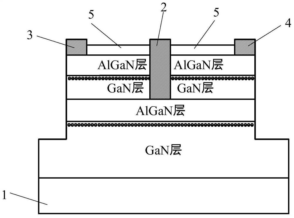
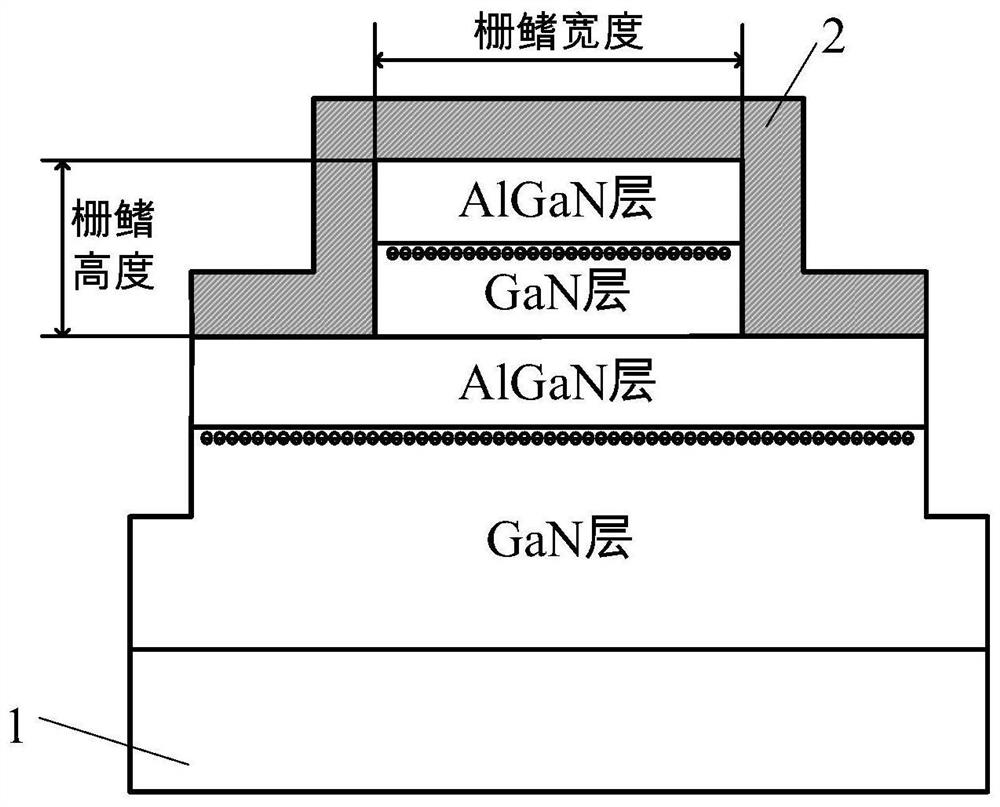
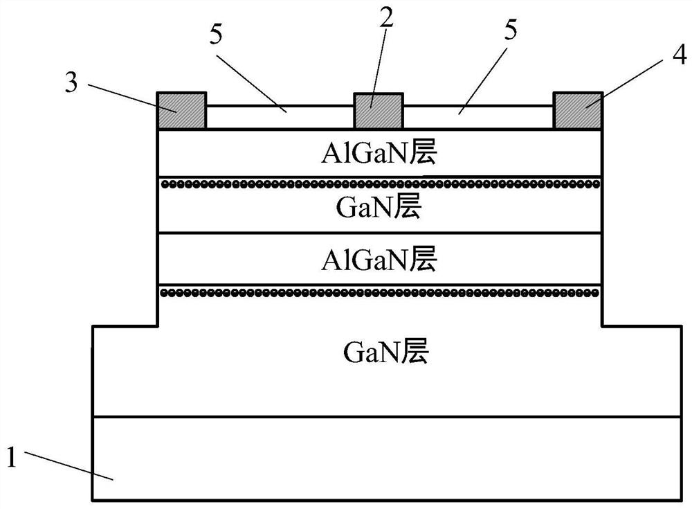
[0048] Please refer to Figure 1-Figure 3 , figure 1 It is a cross-sectional schematic diagram of the outer gate length direction of the gate fin of a GaN transistor device with a high linearity compound gate structure provided by an embodiment of the present invention; figure 2 It is a schematic cross-sectional view of the gate width direction of a GaN transistor device with a high linearity compound gate structure provided by an embodiment of the present invention; image 3 It is a cross-sectional schematic diagram of the internal gate length direction of the gate fin of a GaN transistor device with a high linearity compound gate structure provided by an embodiment of the present invention. As shown in the figure, the high linearity compound gate structure GaN transistor device of this embodiment includes:
[0049] Substrate layer 1;
[0050] a plurality of channel layers, and a plurality of the channel layers are sequentially stacked on the substrate layer 1;
[0051]g...
Embodiment 2
[0065] In this embodiment, a GaN transistor device with a double-channel layer high linearity compound gate structure is used as an example to illustrate the fabrication method thereof. See Figures 4a-4i , Figures 4a-4i It is a schematic process flow diagram of a GaN transistor device with a high linearity compound gate structure provided by an embodiment of the present invention, and the preparation method includes the following steps:
[0066] Step 1: Select sapphire or SiC as substrate layer 1, see Figure 4a ;
[0067] Step 2: On the sapphire substrate or the SiC substrate layer 1, a GaN buffer layer and an AlGaN barrier layer are grown to form an AlGaN / GaN heterojunction as a channel layer, wherein the thickness of the AlGaN layer is 15-25 nm, and the mole of A The score is 25-35%, see Figure 4b ;
[0068] Step 3: Repeat Step 2 to form a double channel layer, see Figure 4c ;
[0069] Step 4: Set up active area mesa isolation on the dual channel layer, see Fig...
Embodiment 3
[0079] In this embodiment, the specific process flow of the preparation method of the second embodiment is described in detail by taking different AlGaN barrier layer thicknesses and different Al compositions as examples.
[0080] 1. The AlGaN barrier layer thickness is 15nm of the double channel layer, in which the Al composition is 35%. The specific preparation steps are as follows:
[0081] Step 1. Epitaxial Material Growth
[0082] 1.1) On the SiC substrate, use the MOCVD process to grow the GaN buffer layer;
[0083] 1.2) On the GaN buffer layer, grow a 15nm thick AlGaN barrier layer, wherein the Al composition is 35%, and form a two-dimensional electron gas 2DEG at the contact position between the GaN buffer layer and the AlGaN barrier layer;
[0084] 1.3) A second layer of 10nm thick GaN buffer layer is grown on the first layer of AlGaN barrier layer;
[0085] 1.4) A second layer of AlGaN barrier layer with a thickness of 15 nm is grown on the second layer of GaN buff...
PUM
| Property | Measurement | Unit |
|---|---|---|
| thickness | aaaaa | aaaaa |
| width | aaaaa | aaaaa |
| thickness | aaaaa | aaaaa |
Abstract
Description
Claims
Application Information
 - R&D
- Intellectual Property
- Life Sciences
- Materials
- Tech Scout
- Unparalleled Data Quality
- Higher Quality Content
- 60% Fewer Hallucinations
Browse by: Latest US Patents, China's latest patents, Technical Efficacy Thesaurus, Application Domain, Technology Topic, Popular Technical Reports.
© 2025 PatSnap. All rights reserved.Legal|Privacy policy|Modern Slavery Act Transparency Statement|Sitemap|About US| Contact US: help@patsnap.com