Transparent conductive film, patterned transparent conductive film, optical member and electronic device
A transparent conductive film and transparent film technology, applied in the direction of optical elements, optics, conductive layers on insulating carriers, etc., can solve problems such as damage to the transparent conductive layer, and achieve the advantages of improving yield, not easy to curl, and reducing coating film defects. Effect
- Summary
- Abstract
- Description
- Claims
- Application Information
AI Technical Summary
Problems solved by technology
Method used
Image

Examples
Embodiment
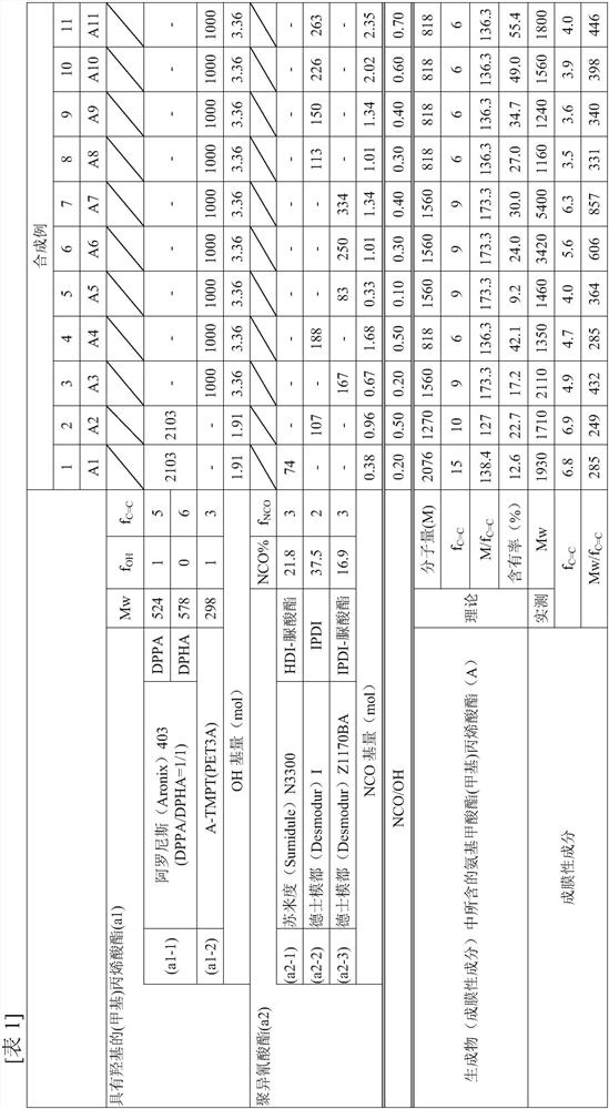
[0164] Hereinafter, although an Example demonstrates this invention, this invention is not limited to the said Example at all. In addition, in the synthesis example and the working example, except for the solvent, the number of prepared materials is in terms of non-volatile components.
[0165] [Determination of molecular weight]
[0166] The mass average molecular weight (Mw) and the number average molecular weight (Mn) are measured by gel permeation chromatography (GPC) method. The measurement conditions are as follows. In addition, both Mw and Mn are values in terms of polystyrene.
[0167] Device: Shimadzu Prominence (SHIMADZU Prominence) (manufactured by Shimadzu Corporation),
[0168] String: Connect three Shodex (SHODEX) LF-804 (manufactured by Showa Denko Co., Ltd.) in series,
[0169] Detector: differential refractive index detector,
[0170] Solvent: tetrahydrofuran (THF, tetrahydrofuran),
[0171] Flow rate: 1.0mL / min,
[0172] Solvent temperature: 40°C,
...
Synthetic example 1
[0177] (A1): In a four-necked flask including a stirrer, a reflux cooler, a nitrogen inlet tube, a thermometer, and a dropping funnel, put Aronix (Aronix) M403: 2103g (containing molecular weight: 524 dipentaerythritol pentaacrylate ( 1000 g (about 1.91 moles) of DPPA) and 1103 g (about 1.91 moles) of dipentaerythritol hexaacrylate (DPHA) with a molecular weight of 578. Toagosei Co., Ltd.), Neostann U-810 (tin catalyst, manufactured by Nitto Chemical Co., Ltd.): 0.1 g, butyl acetate: 815 g, after making the liquid temperature 50° C., hexaethylene oxide containing about 21.8 mass % of isocyanate groups was added dropwise from the dropping funnel over 30 minutes. Urate body of methyl diisocyanate: 74 g (containing about 0.38 mol of isocyanate group). After the heating was completed, the temperature was raised to 80° C. and reacted for 3 hours. After confirming that the peak of the isocyanate group disappeared using a Fourier Transform Infrared Spectrometer (FT-IR), butyl acetate...
Embodiment 1
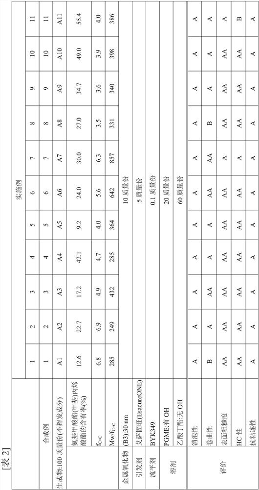
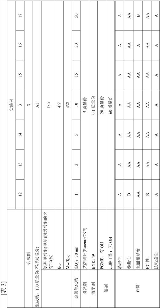
[0192] 100 parts by mass (non-volatile matter) of product A containing urethane (meth)acrylate synthesized in Synthesis Example 1, and 10 parts by mass of (B3) described later as a metal oxide having an average primary particle diameter of 30 nm , Esacure ONE (Esacure ONE) (manufactured by IGM-resins (IGM-Resins) B.V. company) as a photopolymerization initiator 5 parts by mass, BYK349 (silicone-based additives as a leveling agent, Japanese BYK Chemicals (BYK -Chemie Japan) Co., Ltd.) 0.1 parts by mass, 20 parts of polyethylene glycol monoethyl ether (PGME) and 60 parts of butyl acetate as a diluting solvent were mixed and dispersed to obtain a hard coating agent 1.
[0193] The defoaming properties of the hard coat agent, the curling properties of the intermediate laminate provided with the hard coat layer, the surface roughness of the hard coat layer, and the hardness (HC properties) of the hard coat layer were evaluated according to the methods described below.
PUM
| Property | Measurement | Unit |
|---|---|---|
| Surface roughness | aaaaa | aaaaa |
| Surface roughness | aaaaa | aaaaa |
Abstract
Description
Claims
Application Information
 - Generate Ideas
- Intellectual Property
- Life Sciences
- Materials
- Tech Scout
- Unparalleled Data Quality
- Higher Quality Content
- 60% Fewer Hallucinations
Browse by: Latest US Patents, China's latest patents, Technical Efficacy Thesaurus, Application Domain, Technology Topic, Popular Technical Reports.
© 2025 PatSnap. All rights reserved.Legal|Privacy policy|Modern Slavery Act Transparency Statement|Sitemap|About US| Contact US: help@patsnap.com