Titanium dioxide semiconductor film, preparation method and application of titanium dioxide semiconductor film in photoelectrocatalysis
A titanium dioxide and semiconductor technology, applied in the field of optoelectronic semiconductor thin film materials, can solve the problems of low photocurrent density of titanium dioxide thin film, low photoelectric catalytic efficiency, affecting the popularization and application of titanium dioxide thin film, etc. Effect
- Summary
- Abstract
- Description
- Claims
- Application Information
AI Technical Summary
Problems solved by technology
Method used
Image
Examples
Embodiment approach
[0040] The third embodiment of the present invention provides an application of the above-mentioned titanium dioxide semiconductor thin film in photoelectrocatalysis.
[0041] The fourth embodiment of the present invention provides a photoelectric catalytic reactor, including a photoanode, and the active material of the photoanode is the above-mentioned titanium dioxide semiconductor thin film.
[0042] A specific method for the application of titanium dioxide semiconductor thin film in photoelectrocatalysis, for example, providing the photoelectrocatalytic reactor mentioned above to split water to produce hydrogen.
[0043] In order to enable those skilled in the art to understand the technical solution of the present invention more clearly, the technical solution of the present invention will be described in detail below in conjunction with specific examples and comparative examples.
[0044] In a specific embodiment, the target used is a titanium target with a size of 3 inc...
Embodiment 1
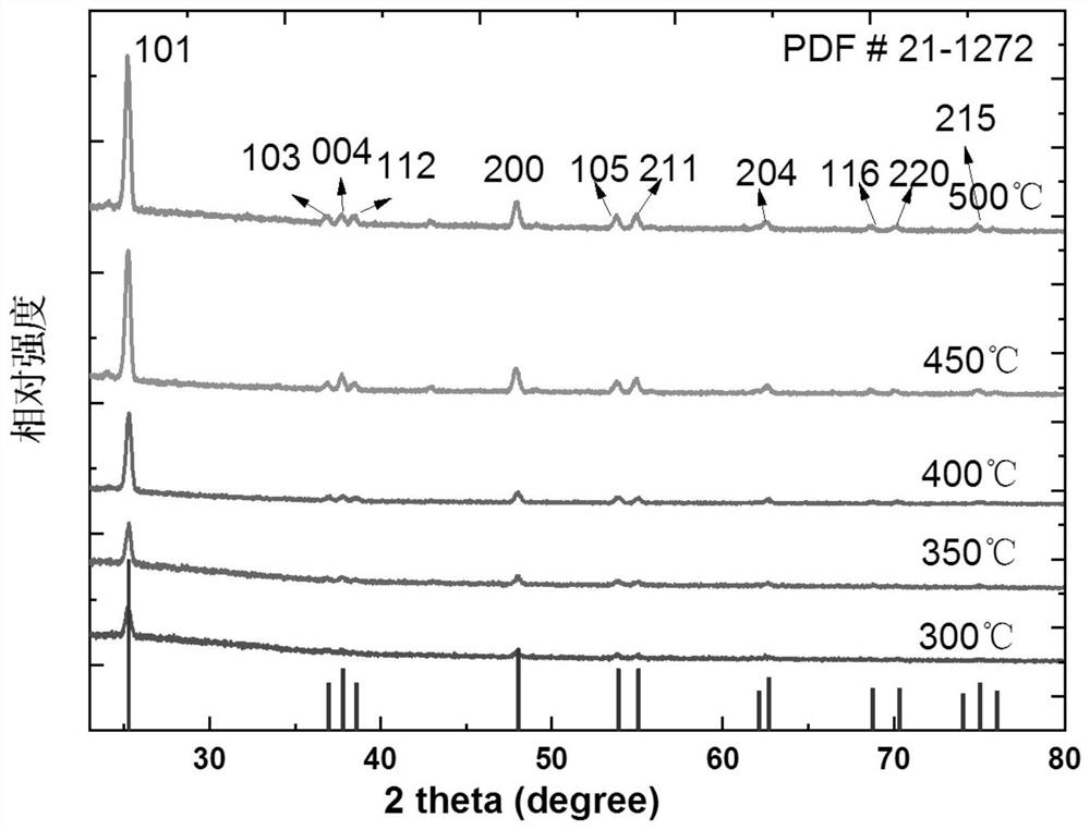
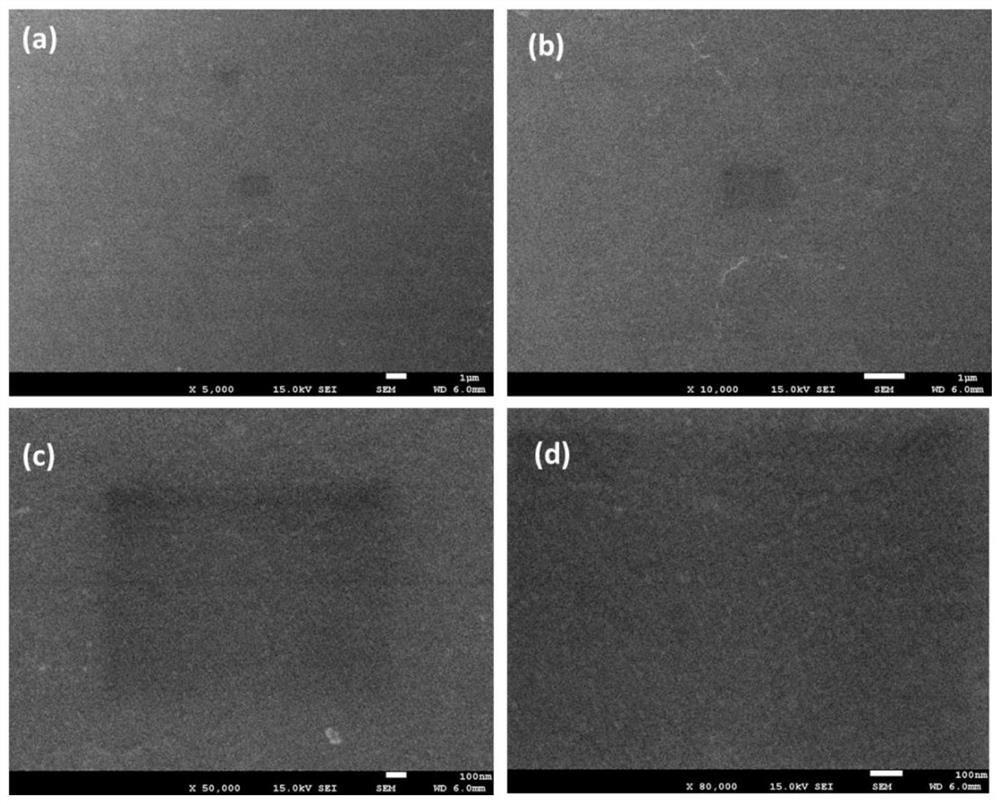
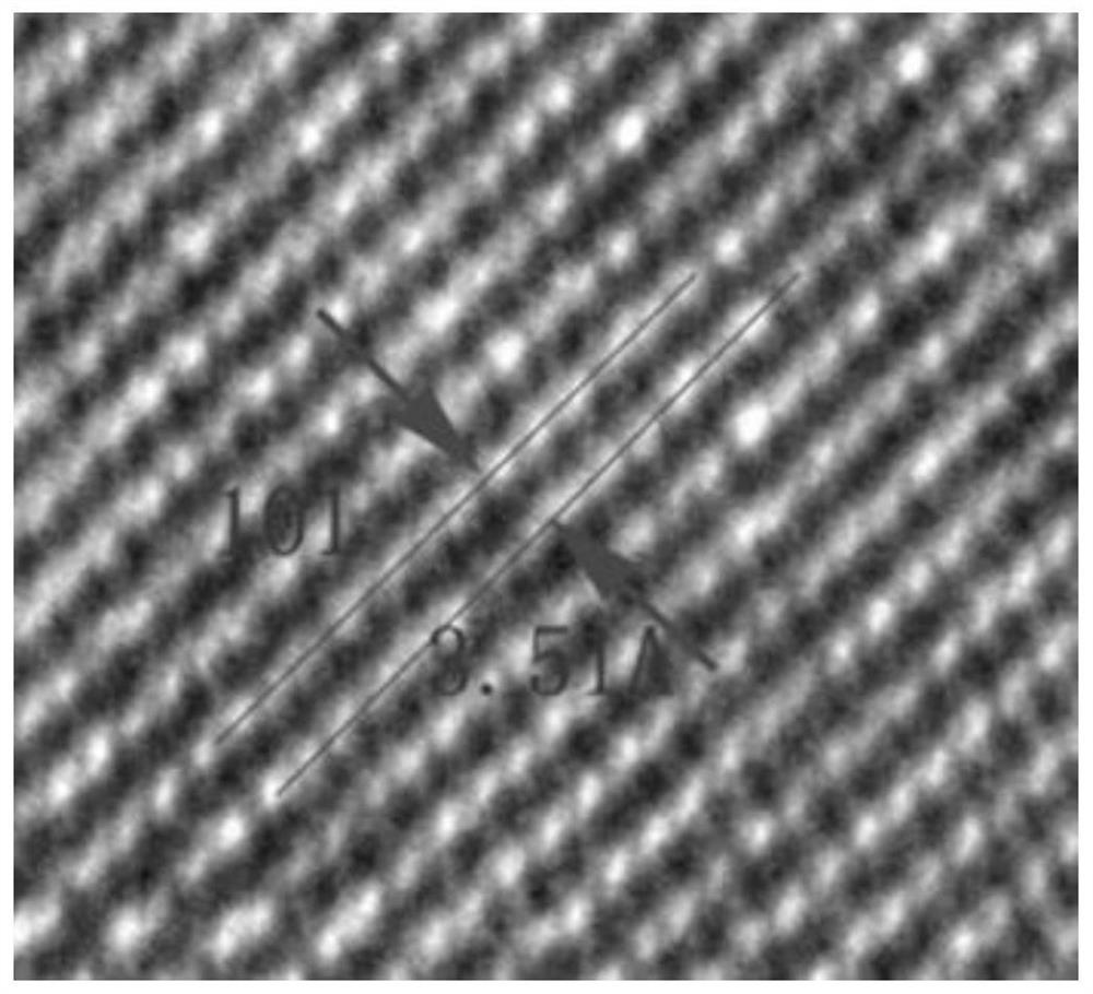
[0046] The anatase TiO of this embodiment 2 The preparation method of thin film, comprises the following steps:
[0047] 1) Cleaning the glass substrate: Put the glass substrate into acetone, isopropanol, ethanol and deionized water in sequence for ultrasonic cleaning, each cleaning time is 20min, and the cleaning temperature is 50°C; Wipe it clean with a dust-free cloth, and finally put it into the sputtering chamber of the remote plasma sputtering system, ready for sputtering;
[0048] 2) Sputtering: Argon is used as the plasma gas source, oxygen is used as the reaction gas, and the remote plasma sputtering technology is used to deposit the thin film on the glass substrate by reactive sputtering, specifically:
[0049] Before reactive sputtering, the sputtering chamber of the remote plasma sputtering system was evacuated to 5×10 -6 mbar, and then 100 sccm of argon gas is introduced into the chamber. After the pressure in the chamber remains stable, the plasma source emissi...
Embodiment 2
[0056] The anatase TiO of this embodiment 2 The preparation method of thin film, comprises the following steps:
[0057] 1) Cleaning the glass substrate: Put the glass substrate into acetone, isopropanol, ethanol and deionized water in sequence for ultrasonic cleaning, each cleaning time is 20min, and the cleaning temperature is 50°C; Wipe it clean with a dust-free cloth, and finally put it into the sputtering chamber of the remote plasma sputtering system, ready for sputtering;
[0058] 2) Sputtering: Argon is used as the plasma gas source, oxygen is used as the reaction gas, and the remote plasma sputtering technology is used to deposit the thin film on the glass substrate by reactive sputtering, specifically:
[0059] Before reactive sputtering, the sputtering chamber of the remote plasma sputtering system was evacuated to 5×10 -6 mbar, and then 100 sccm of argon gas is introduced into the chamber. After the pressure in the chamber remains stable, the plasma source emissi...
PUM
| Property | Measurement | Unit |
|---|---|---|
| diameter | aaaaa | aaaaa |
| thickness | aaaaa | aaaaa |
Abstract
Description
Claims
Application Information
 - R&D
- Intellectual Property
- Life Sciences
- Materials
- Tech Scout
- Unparalleled Data Quality
- Higher Quality Content
- 60% Fewer Hallucinations
Browse by: Latest US Patents, China's latest patents, Technical Efficacy Thesaurus, Application Domain, Technology Topic, Popular Technical Reports.
© 2025 PatSnap. All rights reserved.Legal|Privacy policy|Modern Slavery Act Transparency Statement|Sitemap|About US| Contact US: help@patsnap.com


