Preparation method of silicon carbide N-channel bipolar power device

A power device, bipolar technology, applied in the field of silicon carbide N-channel bipolar power device preparation, can solve the problems of increasing device on-resistance, rough back surface, thick wafer epitaxial wafer, etc., and achieve good ohm Effects of contact, cost savings, and ease of preparation

Inactive Publication Date: 2021-08-24
NO 55 INST CHINA ELECTRONIC SCI & TECHNOLOGYGROUP CO LTD
View PDF0 Cites 1 Cited by
  • Summary
  • Abstract
  • Description
  • Claims
  • Application Information

AI Technical Summary

Problems solved by technology

However, due to the high resistance of the P-type SiC substrate, manufacturing N-channel SiC power devices on the P-type SiC substrate greatly increases the on-resistance of the device and cannot give full play to the advantages of bipolar power devices.
[0005] In order to solve the situation that the resistance of the P-type SiC substrate is too large, a method of using an N-type SiC substrate to fabricate an N-channel insulated gate bipolar transistor (IGBT) device has been proposed. However, in this method, after thinning T

Method used


Image

  • Preparation method of silicon carbide N-channel bipolar power device
  • Preparation method of silicon carbide N-channel bipolar power device
  • Preparation method of silicon carbide N-channel bipolar power device

Examples


Embodiment Construction

[0039] The technical solutions of the present invention will be further described below in conjunction with the accompanying drawings and embodiments.

[0040] The invention provides a method for preparing an N-channel silicon carbide bipolar device by using an N-type silicon carbide substrate to grow epitaxy, through a high-temperature oxidation process, a front-side MOS preparation process, a back-side thinning process, and a laser annealing process. The specific process Proceed as follows:

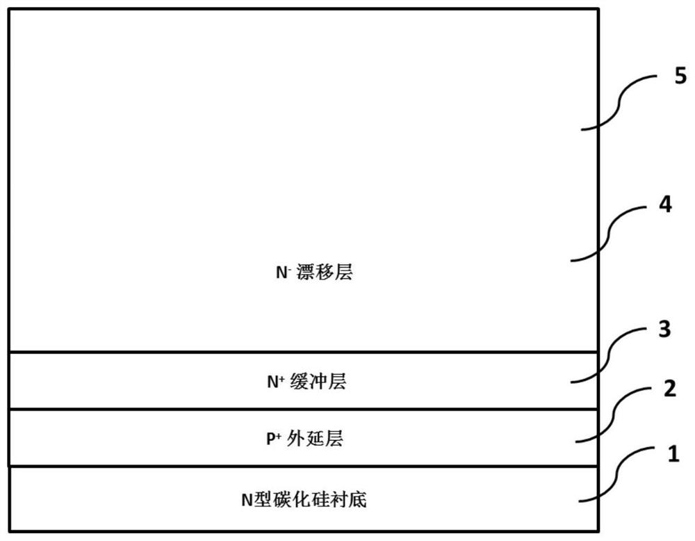
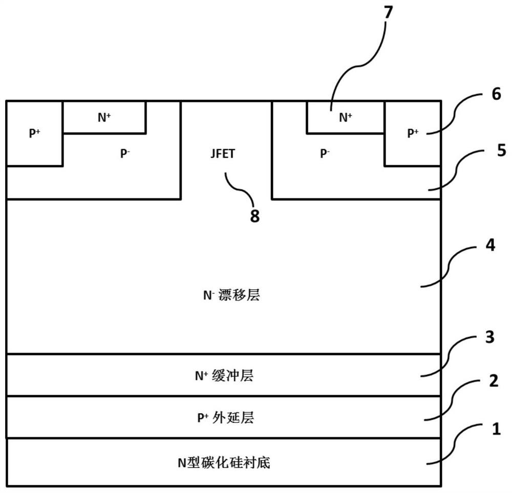
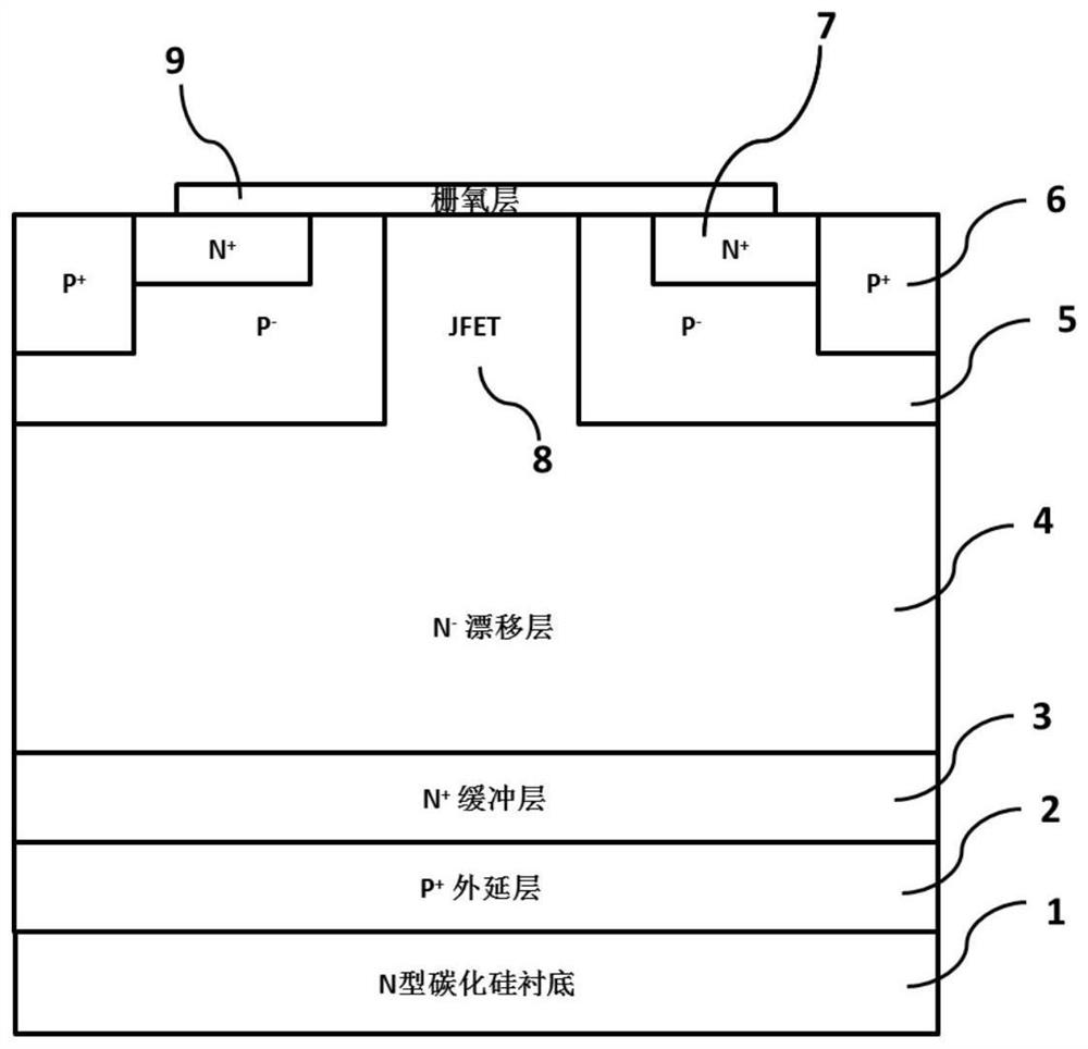
[0041] Step 1, growing P sequentially on the N-type silicon carbide substrate 1 + Epitaxial layer 2, N + Buffer 3 and N - Drift layer 4, such as figure 1 shown. First, epitaxially grow P on the N-type silicon carbide substrate 1 + Epitaxial layer 2, P-type doping concentration is 1e18cm -3 ~1e20cm -3, the thickness is 3μm~30μm; secondly, in P + Epitaxial growth of N on the epitaxial layer 2 + Buffer layer 3, N-type doping concentration is 3e16cm -3 ~3e18cm -3 , the thickness ...


PUM

PropertyMeasurementUnit
Thicknessaaaaaaaaaa
Thicknessaaaaaaaaaa
Thicknessaaaaaaaaaa

Abstract

The invention discloses a preparation method of a silicon carbide N-channel bipolar power device, and belongs to the field of semiconductor devices. According to the method, firstly, a P+ epitaxial layer, an N+ buffer layer and an N- drift layer are sequentially grown on an N-type silicon carbide substrate, secondly, a carrier lifetime prolonging process, a device front MOS preparation process, a device back substrate thinning process and a laser annealing process are introduced on an epitaxial wafer, and finally the preparation of the silicon carbide N-channel bipolar power device is achieved. According to the method, by introducing the carrier lifetime prolonging process, the conductivity modulation effect of the bipolar power device is enhanced, and the specific on-resistance and the conduction loss of the device are effectively reduced. Meanwhile, the method not only avoids the adoption of a high-resistance P-type silicon carbide substrate material, but also has the advantages that the front preparation process of the device is compatible with the preparation process of an MOSFET device, the cost is saved, the risk is smaller, and the industrial preparation is easier.

Description

technical field [0001] The invention relates to a method for preparing a silicon carbide N-channel bipolar power device, belonging to the field of semiconductor devices. Background technique [0002] The development of power electronic devices based on silicon materials has reached a bottleneck period, and it is difficult to meet the requirements of future power electronic systems for rectification and switching devices in terms of ultra-high voltage, high frequency, and high temperature. As the third-generation semiconductor material, silicon carbide semiconductor material not only has three times the forbidden band width of silicon semiconductor material, but also has a critical breakdown electric field 10 times that of silicon material, and has a high electron saturation drift velocity and thermal conductivity, so This makes power devices based on silicon carbide materials have great advantages in the fields of high temperature, high frequency and high power. [0003] Si...

Claims


Application Information

Patent Timeline
IPC IPC(8): H01L21/331H01L21/304H01L21/324H01L21/04H01L29/161
CPCH01L21/0445H01L29/1608H01L29/66068
Inventor 杨晓磊柏松
Owner NO 55 INST CHINA ELECTRONIC SCI & TECHNOLOGYGROUP CO LTD
Why Eureka
Try Eureka