Transition metal nitride coating with nano multilayer structure as well as preparation method and application thereof
A nano-multilayer, transition metal technology, applied in metal material coating process, metal processing equipment, coating and other directions, can solve the problem that PVD coating cannot have both high hardness and toughness and bonding strength of film base, etc. The effect of grain refinement, good controllability and simple preparation process
- Summary
- Abstract
- Description
- Claims
- Application Information
AI Technical Summary
Problems solved by technology
Method used
Image
Examples
preparation example Construction
[0054] The invention also discloses a preparation method of a transition metal nitride coating with a nano-multilayer structure, which comprises the following steps:
[0055] Depositing a nitride bonding layer on the surface of the metal substrate;
[0056] Depositing a nanometer multi-layer nitride functional layer on the surface of the nitride bonding layer;
[0057] The voltages of bias gradient deposition are -20V nm-100V, -20V nm-200V, -20V nm-300V in sequence.
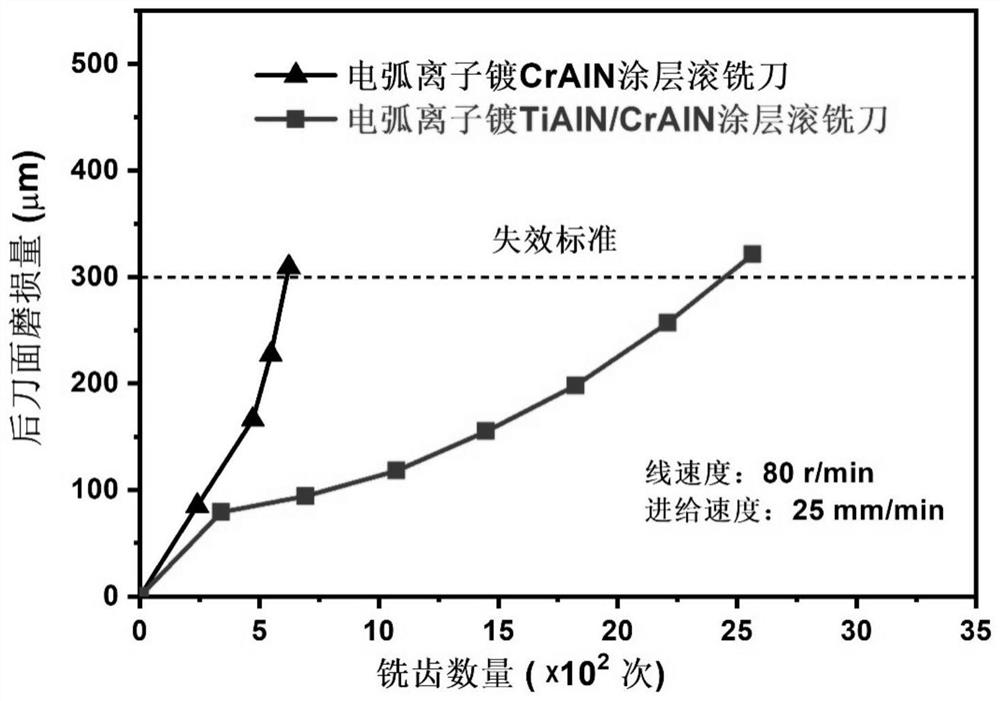
[0058] The metal substrate adopts the hob substrate, and the nanometer multilayer nitride functional layer deposited by arc ion plating on the hob substrate has a modulation period thickness of 3.5nm-80.0nm. In the modulation period, the TiAlN modulation layer and Cr( Al) The modulation ratio of the N layer is 1:10 to 10:1.
[0059] First, the nitride bonding layer is prepared by arc ion plating, and the bonding force between the coating and the substrate is enhanced through the design of the bias gradient, and...
Embodiment 1
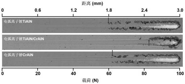
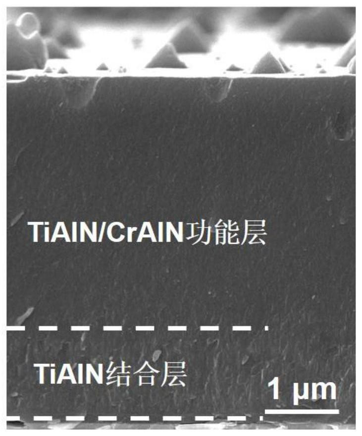
[0074] After the hob is ultrasonically cleaned and dried, it is placed in a coating furnace, and argon and hydrogen are injected. Under the conditions of power of 2.0kW, air pressure of 1.2Pa and increasing bias gradient from -100V to -600V, the tool substrate was ion-etched using the anode layer ion source, and the etching time was 45 minutes. Then turn off the ion source, argon and hydrogen, and after the residual gas is exhausted by the vacuum system, then inject nitrogen, and turn on the arc ion plating TiAl target. The target current is 150A and the bias voltage is -40V~-120V. , the air pressure is 3.5Pa, the rotation rate of the substrate support is 2.0rpm, and the revolution rate is 2.0rpm. The TiAlN bonding layer with a thickness of 1.0 μm is deposited, and the deposition time is 40 minutes; then run the CrAl target at the same time, and adjust the total air pressure to 4.0Pa , the bias voltage is an increasing gradient of -40V to -150V, the CrAl target current is 150A...
Embodiment 2
[0085] After the hob is ultrasonically cleaned and dried, it is sent into the coating furnace and argon gas is introduced. Under the condition of bias voltage of -600V~-1200V and air pressure of 1.0Pa, ion etching was carried out on the tool substrate by glow discharge, and the etching time was 30 minutes. Afterwards, the argon gas is turned off, nitrogen gas is introduced, and the arc ion plating CrAl target is turned on. The target current is 120A, the bias voltage is -40V to -150V, the pressure is 3.0Pa, the rotation rate of the substrate support is 3.0rpm, and the revolution rate is 3.0rpm. Deposit a ~0.5μm thick CrAlN bonding layer under the condition of 2.0rpm, and the deposition time is 20 minutes; then start the TiAl target at the same time, the target current is 100A, the total pressure is 2.5Pa, and the bias voltage is incrementally from -30V to -200V Gradient, under the condition that the rotation rate of the substrate support is 3.0 rpm and the revolution rate is 2...
PUM
| Property | Measurement | Unit |
|---|---|---|
| Etching depth | aaaaa | aaaaa |
| Thickness | aaaaa | aaaaa |
Abstract
Description
Claims
Application Information
 - R&D
- Intellectual Property
- Life Sciences
- Materials
- Tech Scout
- Unparalleled Data Quality
- Higher Quality Content
- 60% Fewer Hallucinations
Browse by: Latest US Patents, China's latest patents, Technical Efficacy Thesaurus, Application Domain, Technology Topic, Popular Technical Reports.
© 2025 PatSnap. All rights reserved.Legal|Privacy policy|Modern Slavery Act Transparency Statement|Sitemap|About US| Contact US: help@patsnap.com


