AgBiS2 film and preparation method and application thereof

A thin-film and soluble technology, which is applied in semiconductor/solid-state device manufacturing, liquid chemical plating, organic semiconductor devices, etc., can solve the problems of preparation phase and singleness, and achieve a shape without holes, low energy consumption, and dense films. Effect

Active Publication Date: 2022-01-11
WUHAN UNIV
View PDF2 Cites 1 Cited by
  • Summary
  • Abstract
  • Description
  • Claims
  • Application Information

AI Technical Summary

Problems solved by technology

[0005]Aiming at the problem that the existing technology cannot prepare AgBiS2 thin films with single phase, high quality and excellent photoelectric device performance by chemical bath deposition method , the present invention pre

Method used


Image

  • AgBiS2 film and preparation method and application thereof
  • AgBiS2 film and preparation method and application thereof
  • AgBiS2 film and preparation method and application thereof

Examples


Embodiment 1

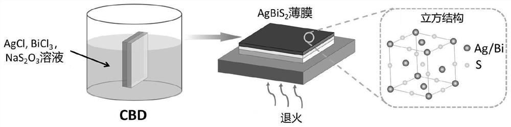
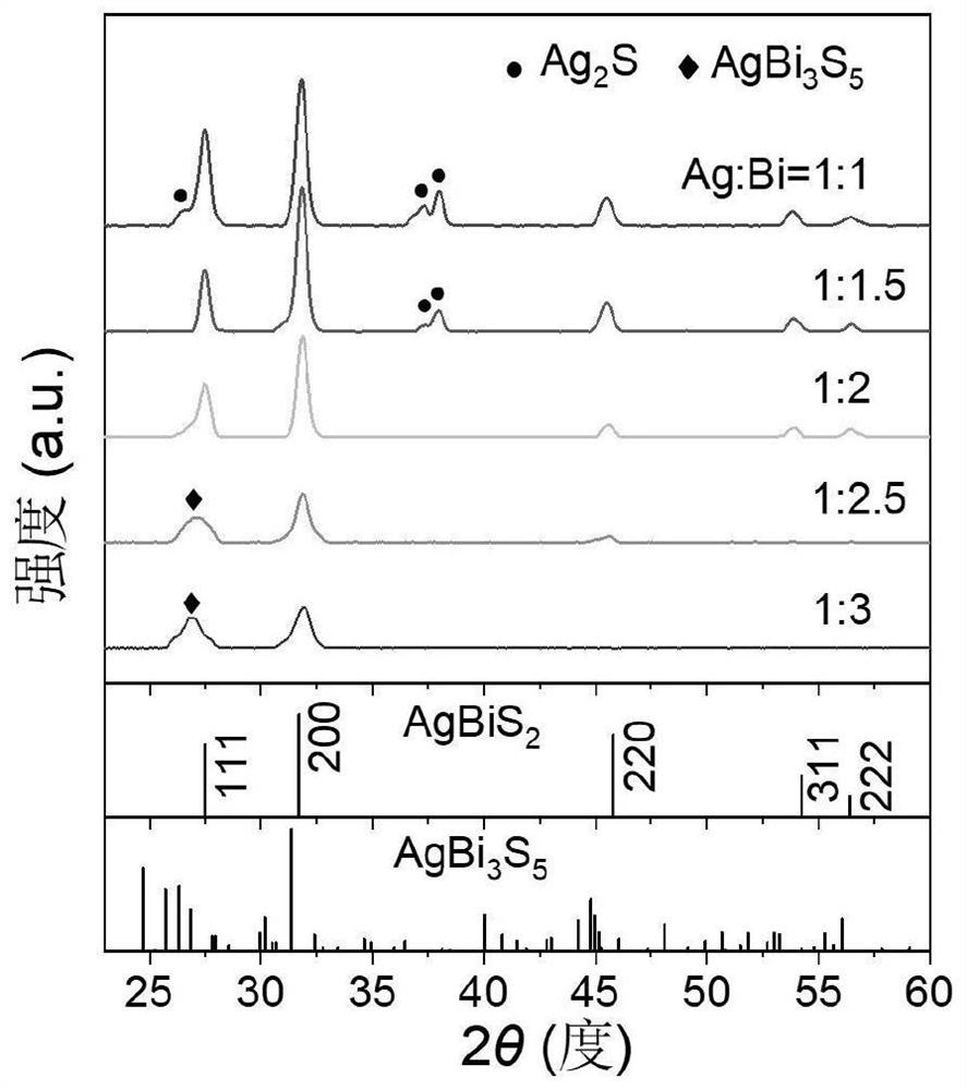
[0036] We first studied Ag 2 S and Bi 2 S 3 film deposition rate, found Ag 2 S grows faster than Bi 2 S 3 much faster. Based on this result, we carefully adjusted the molar ratio of Ag and Bi in the precursor solution.

[0037] (1) AgCl and BiCl were mixed according to Ag and Bi molar ratios of 1:1, 1:1.5, 1:2, 1:2.5, 1:3 respectively 3 dissolved in deionized water (Ag + Concentration is 0.002mol / L), get 5 parts of metal salt aqueous solution;

[0038] (2) Press S 2 o 2 2- Concentration is 0.02mol / L Na 2 S 2 o 2 ·5H 2 O was added to each part of the metal salt aqueous solution, fully stirred until the solid was completely dissolved;

[0039] (3) Adding hydrochloric acid to the solution obtained in step (2) respectively, adjusting the pH value to 3 to obtain a precursor solution;

[0040] (4) Completely immerse the conductive substrates deposited with the CdS thin film by chemical bath deposition in each precursor solution, and maintain the temperature of the pr...

Embodiment 2

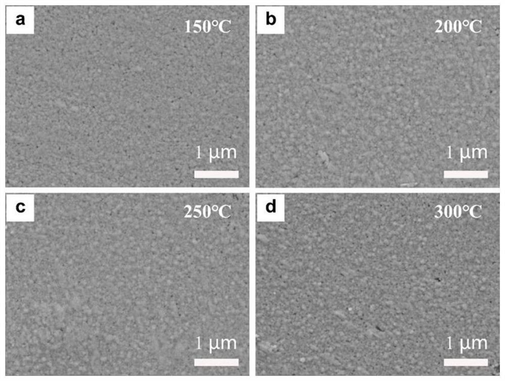
[0044] The preparation AgBiS that this embodiment provides 2 The method of the thin film is basically the same as in Example 1, the only difference is that in this example, the molar ratio of Ag and Bi is controlled to be 1:2, and the annealing temperature (150°C, 200°C, 250°C, 300°C) in step (5) is changed. ℃, 350℃, 400℃).

[0045] Such as image 3 As shown, the higher the annealing temperature, the larger the grain size; Figure 4 As shown, it can be seen from the XRD pattern of the film that AgBiS has formed at 80 °C 2 phase; as the annealing temperature increased to 300 °C, AgBiS 2 The characteristic peaks are obviously enhanced. However, with the further increase of annealing temperature, AgBiS 2 The characteristic peaks decreased significantly, and Ag 5 BiO 4 phase, indicating that AgBiS 2 After the deterioration and degradation of the crystal phase, the composite oxide of Ag and Bi is formed, and the annealing temperature is too high will cause AgBiS 2 High tem...

Embodiment 3

[0047] The preparation AgBiS that this embodiment provides 2 The method of thin film is basically the same as Example 1, and the only difference is that the present embodiment controls the Ag, Bi molar ratio to be 1:2, and changes the time (0.5 hours, 1 hour, 1.5 hours) of static deposition in step (4). ,2 hours). Such as Figure 5 As shown, AgBiS 2 The thickness of the film has a linear relationship with the static deposition time, which proves that the preparation of AgBiS provided by this embodiment 2 Thin-film approach enables precise tuning of AgBiS 2 Thickness of the film. The method provided in this example can prepare AgBiS with a thickness of 90 nm within 2 hours. 2 Compared with the traditional quantum dot preparation method, the preparation efficiency of thin film is greatly improved.


PUM

PropertyMeasurementUnit
Crystal sizeaaaaaaaaaa
Thicknessaaaaaaaaaa

Abstract

The invention relates to an AgBiS2 film and a preparation method and application thereof. The preparation method comprises the following steps that soluble silver salt and soluble bismuth salt are added into water according to the molar ratio of Ag to Bi being 1: 1-3, soluble thiosulfate with the sulfur molar weight not lower than the sum of Ag and Bi is added, after even mixing is conducted, acid is added to adjust the pH value to be 3, and a precursor solution is obtained; in the precursor solution, cations of the soluble thiosulfate, the soluble silver salt, the soluble bismuth salt and anions of acid do not participate in the deposition reaction; a substrate is placed in the precursor solution, standing and depositing are conducted at 80 +/-5 DEG C for at least 30 minutes, and the substrate is taken out; and the substrate is annealed in air at the temperature of 80-300 DEG C to obtain the substrate attached with the AgBiS2 film. The preparation method has the advantages of simplicity in operation, mild reaction conditions, low cost, low requirements on equipment and environment and the like, and the prepared AgBiS2 film is high in quality, good in optical and electrical performance, good in photovoltaic performance and good in detection performance and has great application potential in the photoelectric field.

Description

technical field [0001] The invention relates to the technical field of manufacturing light-absorbing layer materials of photoelectric devices, in particular to an AgBiS 2 Thin films and their methods of preparation and applications. Background technique [0002] ikB 2 It is a non-toxic and abundant material with suitable band gap (~1.1eV) and high UV-NIR absorption coefficient (about 10 5 cm -1 ), is one of the most promising materials in the field of optoelectronics. Based on AgBiS 2 The solar cell of the material exhibits ultra-high stability, achieves a photoelectric conversion efficiency exceeding 6.4%, and shows great application potential in the field of photovoltaics. However, efficient optoelectronic devices are based on AgBiS 2 realized by quantum dots. The synthesis steps of quantum dots are complicated, and a series of engineering such as surface ligand regulation has a great impact on the performance of materials and devices. AgBiS with nanoscale grain si...

Claims


Application Information

Patent Timeline
IPC IPC(8): C23C18/12H01L51/42H01L51/46
CPCC23C18/1204H10K30/30H10K2102/00Y02E10/549Y02P70/50
Inventor 林乾乾姚方江力
Owner WUHAN UNIV
Why Eureka
Try Eureka