Perovskite photovoltaic cell for passivating adjacent interfaces of photosensitive layers by MoS2 nanosheet and preparation method of perovskite photovoltaic cell

A photovoltaic cell and perovskite technology, applied in photovoltaic power generation, nanotechnology, nanotechnology, etc., can solve problems such as the impact of the environment and its carrying capacity, and achieve effective matching, increase migration channels, and reduce accumulation.

Pending Publication Date: 2022-01-28
WUHAN INSTITUTE OF TECHNOLOGY
View PDF0 Cites 0 Cited by
  • Summary
  • Abstract
  • Description
  • Claims
  • Application Information

AI Technical Summary

Problems solved by technology

[0006] However, MoS is usually synthesized by solution method 2 Nanosheets, the synthesized products are affected by the solvent, and the cleaning of the synthesized products requires a large amount of other solvents, which affects the environment and its carrying capacity

Method used


Image

  • Perovskite photovoltaic cell for passivating adjacent interfaces of photosensitive layers by MoS2 nanosheet and preparation method of perovskite photovoltaic cell
  • Perovskite photovoltaic cell for passivating adjacent interfaces of photosensitive layers by MoS2 nanosheet and preparation method of perovskite photovoltaic cell
  • Perovskite photovoltaic cell for passivating adjacent interfaces of photosensitive layers by MoS2 nanosheet and preparation method of perovskite photovoltaic cell

Examples


preparation example Construction

[0060] (2)MoS 2 Preparation of nanomaterials:

[0061] (a) Ball milling: the weighed MoS 2 Put the solid powder into the mortar of the ball mill, add 100ml of isopropanol solution, adjust the rotation speed to 580rad / min, and start grinding for one week.

[0062] (b) Centrifugation: After grinding, the pellets were cleaned with isopropanol solution, and the MoS 2 The solutions were mixed, placed in a centrifuge and centrifuged twice. After the first centrifugation (8000rad / min), the supernatant in the centrifuge tube was taken out, and then the second centrifugation (11000rad / min) was carried out to get the lower layer in the centrifuge tube. precipitation.

[0063] (c) Drying: Put the final precipitate in a 60°C drying oven for 12 hours to obtain MoS 2 Nanosheets.

Embodiment 1

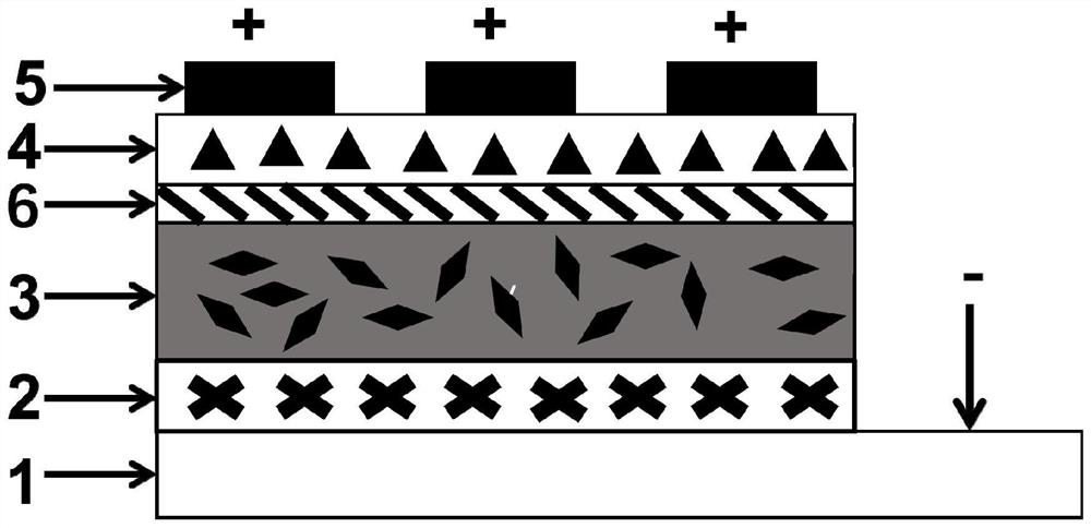
[0065] Such as figure 1 As shown, a planar structure perovskite photovoltaic cell includes a transparent conductive substrate, an electron transport layer, a perovskite photosensitive active layer, an interface passivation layer, a hole transport layer and a metal electrode, and its preparation method includes the following steps:

[0066] (1) Treatment of transparent conductive substrate: cleaning FTO (fluorine-doped SnO 2 ) conductive glass sheet, first soak the conductive glass sheet in a solution containing a cleaning agent (such as Libai brand liquid detergent) for 30 minutes, then repeatedly scrub and rinse with clean water; then polish with polishing powder; then respectively Put it into a vessel containing deionized water, acetone and alcohol and sonicate it for 20 minutes; finally put it in deionized water and rinse it twice, blow dry with a nitrogen gun and put it in an oven at 80°C for drying;

[0067] (2)SnO 2 Preparation of QD thin films: SnO on FTO substrates ...

Embodiment 2

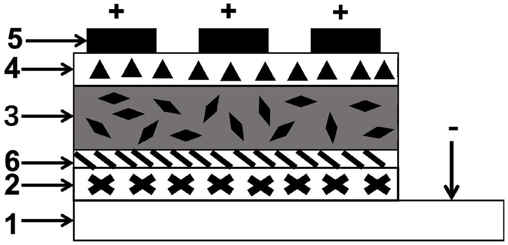
[0078] Such as figure 1 As shown, a planar structure perovskite photovoltaic cell includes a transparent conductive substrate, an electron transport layer, a perovskite photosensitive active layer, an interface passivation layer, a hole transport layer and a metal electrode, and its preparation method includes the following steps:

[0079] (1) cleaning ITO conductive glass sheet: with embodiment 1;

[0080] (2)SnO 2 Thin film preparation: SnO was prepared on ITO substrate by spin coating method (2500rad / min) 2 film, and put it into a UV-ozone cleaner, and treat it with UV-ozone for 15 minutes in an atmospheric atmosphere and at room temperature, and the treated SnO 2 / ITO substrate is quickly transferred into the glove box;

[0081] (3) Preparation of perovskite photosensitive active layer: same as Example 1;

[0082] (4) Prepare an interface passivation layer on the perovskite photosensitive film:

[0083] a. Solution preparation: MoS prepared by ball milling in advance ...


PUM


Abstract

The invention discloses a perovskite photovoltaic cell for passivating adjacent interfaces of photosensitive layers by an MoS2 nanosheet and a preparation method of the perovskite photovoltaic cell. The cell sequentially comprises a transparent conductive substrate, an electron transport layer, a perovskite photosensitive active layer, a hole transport layer and a metal electrode; the cell further comprises an interface passivation layer, wherein the interface passivation layer is a MoS2 nanosheet; the MoS2 nanosheet is prepared by a ball milling method; and the interface passivation layer is located between the electron transport layer and the perovskite photosensitive active layer or between the perovskite photosensitive active layer and the hole transport layer. The MoS2 nanosheet obtained through a simple ball milling method has a large specific surface area and mesopores, contact between the MoS2 nanosheet and a perovskite photosensitive layer and an interface layer is effectively enlarged, migration channels of carriers are increased, accumulation of the carriers at the interface is reduced, the extraction rate of the interface layer to the carriers is balanced, and interface recombination is reduced, so that the interface regulation and control technology with high efficiency, long service life, low cost, good stability and high efficiency and a corresponding photovoltaic device are developed.

Description

technical field [0001] The invention belongs to the field of thin film materials and devices, in particular to a two-dimensional material MoS 2 A perovskite photovoltaic cell with a nanosheet passivation interface between a hole transport layer / photosensitive layer or an electron transport layer / photosensitive layer and a preparation method thereof. Background technique [0002] Until 2021, the maximum efficiency of perovskite photovoltaic cells (PSCs) has exceeded 25% (https: / / www.nrel.gov / pv / cell-efficiency.html), and the stability is greatly affected during the commercial development process. focus on. In order to improve the efficiency and stability of battery devices, in addition to preparing high-quality perovskite photosensitive layers, appropriate interface modification and passivation (including electron / hole transport interface layer preparation, doping and related interface modification, etc.) It is very important in the process of device preparation and researc...

Claims


Application Information

Patent Timeline
Patent Type & Authority Applications(China)
IPC IPC(8): H01L51/44H01L51/46H01L51/42H01L51/48B82Y30/00B82Y40/00
CPCB82Y30/00B82Y40/00H10K71/00H10K71/311H10K30/30H10K30/88H10K2102/00Y02E10/549
Inventor 秦平力肖岚王梓逸石畅余雪里马良陈相柏
Owner WUHAN INSTITUTE OF TECHNOLOGY
Why Eureka
Try Eureka