Flexible antimony selenide solar cell and preparation method thereof
A technology of solar cells and antimony selenide, which is applied in circuits, photovoltaic power generation, electrical components, etc., can solve problems such as unfavorable substrates, and achieve the effects of low cost, low equipment cost, and flexible preparation
- Summary
- Abstract
- Description
- Claims
- Application Information
AI Technical Summary
Problems solved by technology
Method used
Image
Examples
Embodiment 1
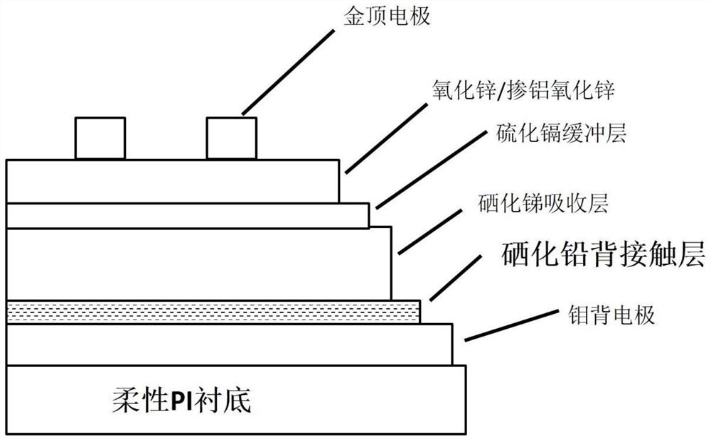
[0021] like figure 1 As shown, the structure of the flexible antimony selenide solar cell provided by the present invention is, from bottom to top, a substrate, a back electrode, a lead selenide back contact layer, an antimony selenide absorption layer, a buffer layer, a window layer and a top electrode. The lead selenide back contact layer is prepared by a low-temperature magnetron sputtering method, and the antimony selenide absorption layer is prepared by a near-space sublimation method. In this embodiment, the substrate is a flexible polyimide PI substrate, the back electrode is a molybdenum back electrode, the buffer layer is a cadmium sulfide buffer layer, the window layer is a zinc oxide / aluminum-doped zinc oxide layer, and the top electrode is a gold electrode.
Embodiment 2
[0023] In this embodiment, the substrate is selected as a polyimide PI substrate coated with a molybdenum back electrode, the sputtering process is selected as a radio frequency magnetron sputtering process, and the sputtering power density is 1.1W / cm 2 , the sputtering target is a circular target with a diameter of 7.62cm, the target is a lead selenide target that meets the stoichiometric ratio, Ar gas is selected as the sputtering gas, and the distance from the target to the substrate is 8cm. The air pressure was set to 0.5Pa, the substrate temperature was set to normal temperature, and the thickness of the prepared lead selenide film was set to 5nm.
[0024] After the preparation of the lead selenide film is completed, a near-space sublimation process is applied to prepare an antimony selenide absorption layer on the lead selenide. The substrate temperature was set to 300°C, the evaporation source temperature was set to 510°C, and the thickness of the prepared antimony sele...
Embodiment 3
[0029] The lead selenide back contact layer prepared by the invention is used to prepare a flexible antimony selenide solar cell, the structure of which is a flexible polyimide substrate / molybdenum back electrode / lead selenide back contact layer / antimony selenide absorption layer / cadmium sulfide buffer layer / zinc oxide / aluminum doped zinc oxide window layer / gold top electrode (e.g. figure 1 shown)
[0030] The specific preparation steps are as follows:
[0031] (1) Cleaning the substrate
[0032] The flexible polyimide was used as the substrate, and the surface of the polyimide was washed successively with electronic cleaning agent, absolute ethanol and deionized water, and then the surface of the substrate was dried with nitrogen.
[0033] (2) Preparation of molybdenum back electrode
[0034] The Mo back electrode was prepared by DC magnetron sputtering technology, and the sputtering power density of the target was 3.9W / cm 2 , the sputtering pressure is 0.3Pa, the thickne...
PUM
| Property | Measurement | Unit |
|---|---|---|
| thickness | aaaaa | aaaaa |
| thickness | aaaaa | aaaaa |
| thickness | aaaaa | aaaaa |
Abstract
Description
Claims
Application Information


