Optically transparent nonvolatile transistor memory and preparation method thereof
An optically transparent and non-volatile technology, applied in the field of memory, can solve the problems of poor process continuity and high price, and achieve the effects of good working reliability and working stability, low preparation cost and good repeatability
- Summary
- Abstract
- Description
- Claims
- Application Information
AI Technical Summary
Problems solved by technology
Method used
Image
Examples
preparation example Construction
[0030] The present invention also provides a method for preparing an optically transparent nonvolatile transistor memory described in the above technical solution, comprising the following steps:
[0031] (1) Commercially purchased glass with patterned indium tin oxide, polyethylene terephthalate, polyethylene naphthalate, polyethersulfone, etc. as a substrate; on the substrate, Patterned indium tin oxide thin film as source-drain electrodes;
[0032](2) configure the polymer semiconductor solution, prepare the polymer semiconductor layer with the solution method (spin coating, scraping, drop coating) process on the surface of the source-drain electrode of the step (1); then heat treat the semiconductor layer , to remove the residual solvent in the polymer semiconductor layer, the temperature of the heat treatment is preferably 60-120°C; the time is preferably 10-120 minutes; the concentration of the polymer semiconductor solution is preferably 0.2%-1% by mass; The adjustment...
Embodiment 1
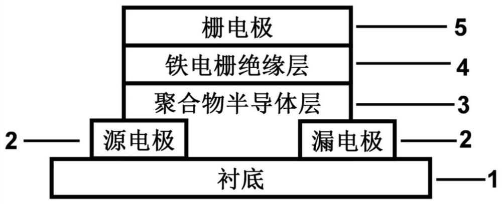
[0039] This embodiment provides an optically transparent non-volatile transistor memory, which is a top-gate structure, and is composed of a substrate, a source-drain electrode, a polymer semiconductor layer, a ferroelectric gate insulating layer and a gate electrode in sequence from bottom to top .
[0040] Wherein, the substrate is glass covered with patterned indium tin oxide, which is purchased from the market; the source-drain electrode is indium tin oxide with a thickness of 50 nanometers; the polymer semiconductor layer is poly{2,2'-[(2, 5-bis(2-octyldodecyl)-3,6-dioxy-2,3,5,6-tetrahydropyrrole[3,4-c]pyrrole-1,4-diacyl)] Dithiophenyl-5,5'-diacylthiophene[3,2-b]thiophene-2,5-diacyl} film with a thickness of 40 nanometers; the ferroelectric grid insulating layer is poly(vinylidene fluoride-trifluoro Polyethylene) film with a thickness of 650 nanometers; the gate electrode is a poly(3,4-ethylenedioxythiophene)-polystyrene sulfonate film with a thickness of 170 nanometers....
Embodiment 2
[0048] This embodiment provides an optically transparent non-volatile transistor memory, which is a top-gate structure, which consists of a substrate, a source-drain electrode, a polymer semiconductor layer, a ferroelectric gate insulating layer, and a gate electrode in sequence from bottom to top. composition.
[0049] Wherein, the substrate is polyethylene terephthalate covered with patterned indium tin oxide, which is purchased from the market; the source-drain electrodes are patterned indium tin oxide films with a thickness of 120 nanometers; the polymer semiconductor layer is poly[(5-fluoro-2,1,3-benzothiazole-4,7-diacyl)(4,4-hexadecyl-4H-cyclopenta[2,1-b:3,4 -b']dithiophene-2,6-diacyl)(6-fluoro-2,1,3-benzothiadiazole)-4,7-diacyl)(4,4-hexadecyl- 4H-Cyclopentane[2,1-b:3,4-b']dithiophenyl-2,6-diacyl)] film with a thickness of 130 nm; the ferroelectric gate insulating layer is vinylidene fluoride- The trifluoroethylene-trifluorochloroethylene copolymer film has a thickness...
PUM
| Property | Measurement | Unit |
|---|---|---|
| thickness | aaaaa | aaaaa |
| thickness | aaaaa | aaaaa |
| thickness | aaaaa | aaaaa |
Abstract
Description
Claims
Application Information
 - R&D
- Intellectual Property
- Life Sciences
- Materials
- Tech Scout
- Unparalleled Data Quality
- Higher Quality Content
- 60% Fewer Hallucinations
Browse by: Latest US Patents, China's latest patents, Technical Efficacy Thesaurus, Application Domain, Technology Topic, Popular Technical Reports.
© 2025 PatSnap. All rights reserved.Legal|Privacy policy|Modern Slavery Act Transparency Statement|Sitemap|About US| Contact US: help@patsnap.com


