Eureka AIR delivers breakthrough ideas for toughest innovation challenges, trusted by R&D personnel around the world.

Texturing and cleaning method of silicon wafer and preparation method of crystalline silicon solar cell

A technology for making texture and silicon wafers, which is applied in the direction of cleaning methods using liquids, cleaning methods and utensils, chemical instruments and methods, etc., and can solve the problem of high unit consumption

Pending Publication Date: 2022-03-29
TONGWEI SOLAR (ANHUI) CO LTD
View PDF0 Cites 2 Cited by
  • Summary
  • Abstract
  • Description
  • Claims
  • Application Information

AI Technical Summary

Problems solved by technology

[0006] Based on this, it is necessary to address the problem of high unit consumption of chemicals such as hydrogen peroxide and hydrochloric acid in the traditional technology, and provide a method for cleaning silicon wafers and a method for preparing crystalline silicon solar cells.

Method used


Image

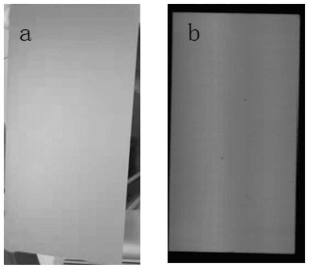
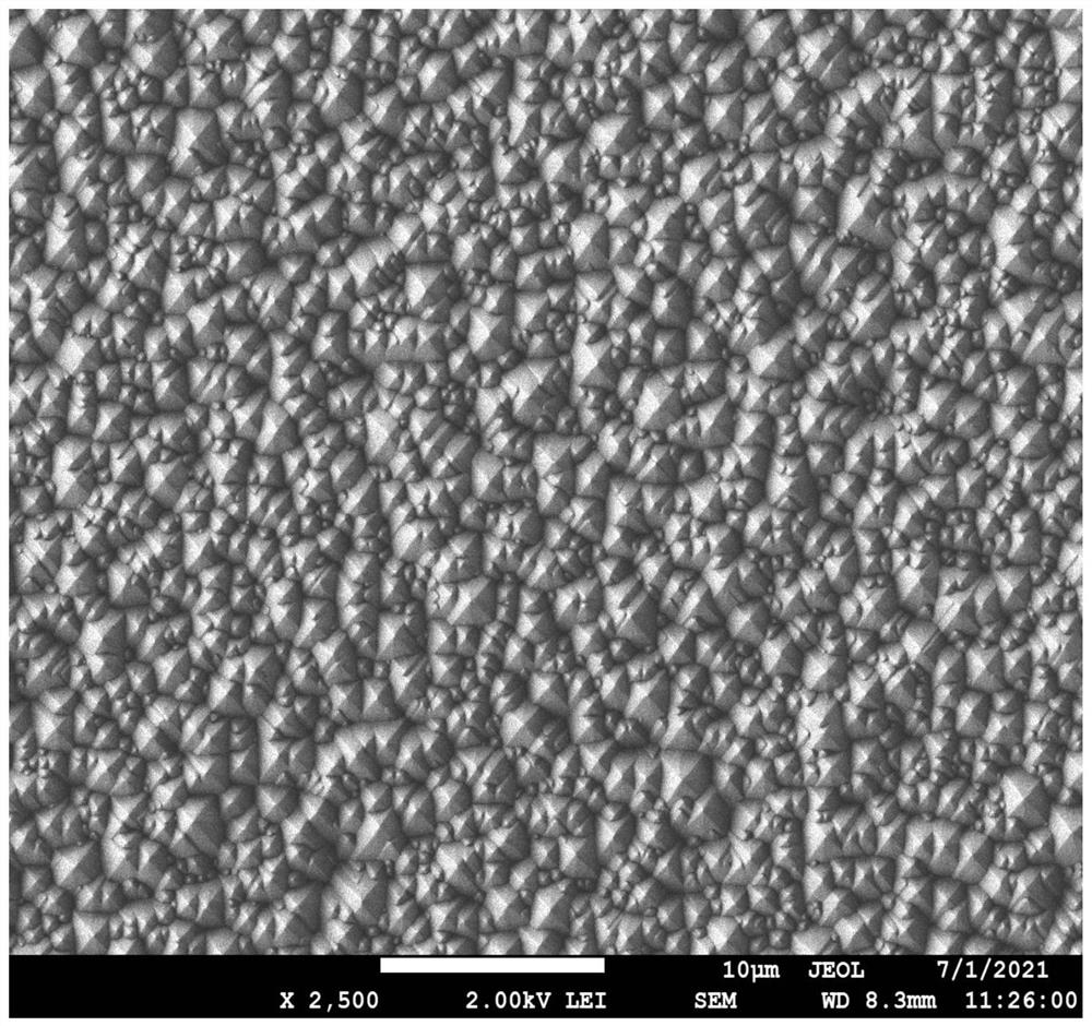
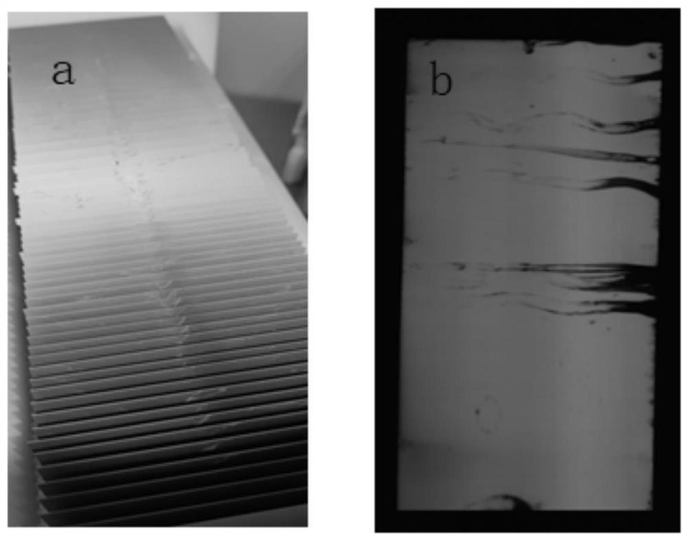
  • Texturing and cleaning method of silicon wafer and preparation method of crystalline silicon solar cell
  • Texturing and cleaning method of silicon wafer and preparation method of crystalline silicon solar cell
  • Texturing and cleaning method of silicon wafer and preparation method of crystalline silicon solar cell

Examples


preparation example Construction

[0088] The present invention also provides a method for preparing a crystalline silicon solar cell, which includes the steps of the above-mentioned texturing and cleaning method for silicon wafers, and after the texturing and cleaning, further includes sequentially depositing an amorphous silicon film and depositing a transparent conductive oxide Thin films and steps for making metal electrodes.

[0089] In some of the embodiments, the above-mentioned crystalline silicon solar cells are HJT cells. Specifically, its crystalline silicon solar cell includes the following steps:

[0090] Thin intrinsic amorphous silicon film (i-a-Si:H) and p-type amorphous silicon film (p-a-Si:H) are deposited on the front side of N-type monocrystalline silicon wafer (c-Si), and then deposited on the silicon wafer Thin intrinsic amorphous silicon film (i-a-Si:H) and n-type amorphous silicon film (n-a-Si:H) are deposited on the back of the wafer to form the back surface field; then transparent oxi...

Embodiment 1

[0095] S1: Coarse throwing. The reagent used for rough throwing is KOH aqueous solution with a mass concentration of 5%, the temperature is set at 80°C, the time is 180s, and the circulation flow rate is kept at about 35L / min. The function is to remove the damaged layer on the surface of the silicon wafer. At this time, the etching depth of the single side of the silicon wafer is about 4 μm.

[0096] S2: pickling (ozone cleaning). The mass concentration of HCl in the pickling solution is 0.02%, the mass concentration of HF is 1%, ozone (O 3 ) concentration is set to 30ppm, the temperature is set to 25°C, the time is set to 240s, 35L / min.

[0097] S3: pre-cleaning (first alkaline washing). The first alkaline washing solution is KOH, H 2 o 2 aqueous solution, wherein the mass concentration of KOH is 1.1%, H 2 o 2 The mass concentration is 4.5%, the temperature is set at 65°C, the time is set at 240s, and the circulation flow is kept at about 40L / min. The function is to r...

Embodiment 2~4

[0106] The steps of Examples 2-4 are the same as those of Example 1, except that the concentrations of reagents used in each step and the temperature, time and flow rate of treatment are adjusted, as shown in Table 1 for details.


PUM


Abstract

The invention relates to a silicon wafer texturing and cleaning method and a preparation method of a crystalline silicon solar cell. The silicon wafer texturing and cleaning method comprises the following steps: sequentially carrying out rough polishing treatment, acid washing treatment, first alkali washing treatment, texturing treatment, second alkali washing treatment, smoothing treatment, passivating treatment and drying treatment on a silicon wafer; a pickling solution used in the pickling treatment contains ozone, HCl and HF; a first alkali wash solution used in the first alkali wash treatment contains soluble alkali metal hydroxide salt and H2O2. The acid washing treatment and the first alkali washing treatment which are sequentially carried out are added between the rough polishing treatment and the texturing treatment; the combination of hydrogen peroxide and hydrochloric acid can greatly improve the cleaning effect, so that a post-cleaning step between subsequent smooth treatment and passivation treatment can be omitted, the consumption of hydrogen peroxide and hydrochloric acid is greatly reduced, the production cost is saved, and meanwhile, the efficiency of the technological process has no obvious difference.

Description

technical field [0001] The invention relates to the technical field of crystalline silicon solar cells, in particular to a texturing and cleaning method for silicon wafers and a preparation method for crystalline silicon solar cells. Background technique [0002] Crystalline silicon solar cells are solar cells based on silicon wafers. Texturing silicon wafers is the first process for manufacturing crystalline silicon cells, also known as "surface texturing". The effective textured structure can make incident light reflect and refract multiple times on the surface of silicon wafers, increasing the light absorption rate , which reduces the reflectivity and helps to improve the performance of the battery. [0003] Heterojunction cells, also known as HJT cells (Hereto-junction with Intrinsic Thin-layer), are known as the most promising solar cell technology after PERC (Passivated Emitter and Rear Cell). Compared with the traditional crystalline silicon technology, due to the i...

Claims


Application Information

Patent Timeline
Patent Type & Authority Applications(China)
IPC IPC(8): H01L31/18H01L21/02H01L31/0236B08B3/08
CPCH01L31/1804H01L21/02068H01L31/02363B08B3/08Y02E10/50Y02P70/50
Inventor 张乔林周守亮王永洁余义苏世杰
Owner TONGWEI SOLAR (ANHUI) CO LTD
Why Eureka
Eureka Blog
Learn More