A kind of LED epitaxial wafer, epitaxial growth method and LED chip

An LED epitaxial wafer and epitaxial growth technology, which is applied in semiconductor devices, electrical components, circuits, etc., can solve the problems of low luminous efficiency of ultraviolet light-emitting diodes, and achieve the effect of enhancing surface mobility, stable luminous efficiency, and reducing trapping.

Active Publication Date: 2022-06-17
JIANGXI ZHAO CHI SEMICON CO LTD
View PDF9 Cites 0 Cited by
  • Summary
  • Abstract
  • Description
  • Claims
  • Application Information

AI Technical Summary

Problems solved by technology

[0005] Based on this, the object of the present invention is to provide an LED epitaxial wafer, an epitaxial growth method and an LED chip, aiming at solving the problem of low luminous efficiency of existing ultraviolet light emitting diodes

Method used


Image

  • A kind of LED epitaxial wafer, epitaxial growth method and LED chip
  • A kind of LED epitaxial wafer, epitaxial growth method and LED chip
  • A kind of LED epitaxial wafer, epitaxial growth method and LED chip

Examples


Embodiment 1

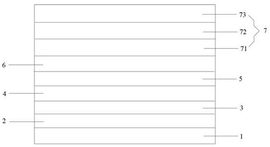
[0031] see figure 1 and figure 2 , shows the LED epitaxial wafer in the first embodiment of the present invention, including a sapphire substrate 1, and an AlN buffer layer 2 epitaxially grown on the sapphire substrate 1 in turn, a three-dimensional island-shaped AlN growth layer 3, and two-dimensional recovery AlN growth layer 4 , n-type AlGaN layer 5 , multiple quantum well layer 6 and p-type layer 7 .

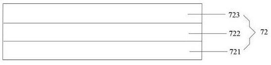
[0032] In this embodiment, the P-type layer 7 is a structure formed by sequentially growing an electron blocking layer 71 , a transition layer 72 and a contact layer 73 , wherein the transition layer 72 is a first sub-layer 721 grown on the electron blocking layer 71 in sequence. , the second sub-layer 722 and the third sub-layer 723. It should be noted that the first sub-layer 721 is P-Al 1-x Sc x N layer, the second sublayer 722 is a GaN layer, and the third sublayer 723 is N-Al 1-y Scy For the N layer, since the growth process of the epitaxial layer generally grows g...

Embodiment 2

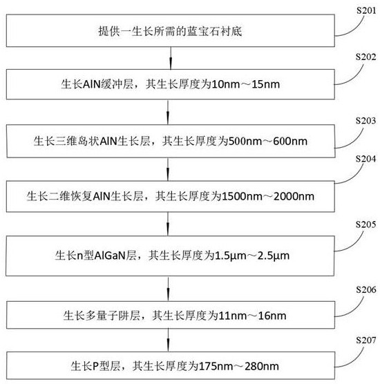
[0036] see image 3 , shows an epitaxial growth method of an LED epitaxial wafer proposed in the second embodiment of the present invention, which is used to prepare the LED epitaxial wafer in the above-mentioned first embodiment. The method specifically includes steps S201 to S207, wherein:

[0037] Step S201, providing a sapphire substrate required for growth.

[0038] In this embodiment, the substrate is a patterned sapphire substrate, which has the advantages of mature technology and low cost. It is an example but not a limitation. In some preferred embodiments of this embodiment, the substrate may also be a Si substrate or SiC substrate.

[0039] In addition, before the growth process, the surface of the substrate needs to be cleaned to avoid doping impurities into the epitaxial wafer, which is beneficial to improve the growth quality of the epitaxial wafer. The specific process of cleaning is to introduce the substrate into the MOCVD reaction chamber, Annealing in a hy...

Embodiment 3

[0065] The third embodiment of the present invention provides an LED chip, including the LED epitaxial wafer in the first embodiment. The LED epitaxial wafer can be epitaxially grown by the epitaxial growth method of the LED epitaxial wafer in the second embodiment.


PUM

PropertyMeasurementUnit
thicknessaaaaaaaaaa
thicknessaaaaaaaaaa
thicknessaaaaaaaaaa

Abstract

The invention provides an LED epitaxial wafer, an epitaxial growth method, and an LED chip. The LED epitaxial wafer includes a P-type layer, the P-type layer includes an electron blocking layer, a transition layer and a contact layer, and the transition layer includes a first sublayer and is sequentially deposited on the second sublayer. Second and third sublayers on one sublayer, first sublayer is P‑Al 1‑x sc x N layer, second sublayer is GaN layer, third sublayer is N‑Al 1‑y sc y N layers. In the present invention, the first sublayer and the third sublayer respectively form a heterojunction interface with the second sublayer, and opposite positive and negative piezoelectric polarization charge densities are generated at the heterojunction interface, which will cause a large number of Non-equilibrium holes are injected into the first sublayer, and then injected into the active region to undergo radiative recombination with electrons, which alleviates the situation of less hole generation due to the high acceptor activation energy of the P-type layer, and solves the problem of ultraviolet light-emitting diodes. The problem of low luminous efficiency.

Description

technical field [0001] The invention relates to the technical field of LEDs, in particular to an LED epitaxial wafer, an epitaxial growth method and an LED chip. Background technique [0002] Light Emitting Diode (LED) is a semiconductor electronic component that can emit light. Due to its small size, high brightness, and low energy consumption, it has attracted more and more researchers' attention. Among them, ultraviolet LEDs The light source has the advantages of high efficiency and energy saving, small size, safety and durability, mercury-free environmental protection, low operating voltage and low power consumption, etc., and is currently widely used in the disinfection of drinking water, disinfection of medical equipment and household appliances, wastewater treatment, plant lighting and other fields. [0003] At present, UV LED epitaxial wafers usually include a substrate and an AlN buffer layer on the substrate, a three-dimensional island-shaped AlN growth layer, a tw...

Claims


Application Information

Patent Timeline
Patent Type & Authority Patents(China)
IPC IPC(8): H01L33/14H01L33/02H01L33/00
CPCH01L33/14H01L33/025H01L33/007
Inventor 胡加辉刘春杨吕蒙普金从龙顾伟
Owner JIANGXI ZHAO CHI SEMICON CO LTD
Why Eureka
Try Eureka