Gallium antimonide wafer processing method

A processing method and technology of gallium antimonide, which is applied in the field of compound semiconductor wafer corrosion process, can solve the problems of reduced wafer value, wafer loss, waste of manpower and material resources, etc., and achieves controllable corrosion process, prevention of twinning distribution, and smooth and bright surface. Effect

Pending Publication Date: 2022-04-01
广东先导微电子科技有限公司
View PDF0 Cites 0 Cited by
  • Summary
  • Abstract
  • Description
  • Claims
  • Application Information

AI Technical Summary

Problems solved by technology

However, during the processing of gallium antimonide wafers, the twins on the wafer surface can only be observed after cleaning. On the one hand, the wafer will be degraded and the value of the wafer will be greatly reduced; on the other hand, the wafer needs to be re-cut for processing and shipping.
Therefore, can cause the loss of wafer and the waste of manpower and material resources
Although there is an EPD etching process for gallium antimonide in the prior art, the function of this process is focused on the identification of dislocations and defects, and it is impossible to identify twins well.

Method used


Image

  • Gallium antimonide wafer processing method

Examples


Embodiment 1

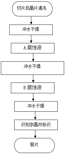
[0028] A processing method for a gallium antimonide wafer, comprising the following steps:

[0029] (1) Clean the sliced ​​gallium antimonide wafer in alcohol to remove the cutting fluid on the surface;

[0030] (2) Rinse the surface of the gallium antimonide wafer with water and dry it after rinsing;

[0031] (3) Soak and corrode the dried gallium antimonide wafer in an etching solution with a mass ratio of sodium hypochlorite and sodium hydroxide of 2 for 50 seconds, clean the wafer with deionized water and dry it;

[0032] (4) After cleaning and drying, put the wafer into the corrosion solution with a volume ratio of hydrofluoric acid and acetic acid of 1 and soak for 30s;

[0033] (5) Then rinse the gallium antimonide wafer surface with deionized water and dry the gallium antimonide wafer to obtain a smoother and brighter wafer;

[0034] (6) Observe the twins on the surface of gallium antimonide wafer under fluorescent lamp and mark the distribution of twins;

[0035] (...

Embodiment 2

[0037] A processing method for a gallium antimonide wafer, comprising the following steps:

[0038] (1) Clean the sliced ​​gallium antimonide wafer in alcohol to remove the cutting fluid on the surface;

[0039] (2) Rinse the surface of the gallium antimonide wafer with water and dry it after rinsing;

[0040] (3) Soak and corrode the dried gallium antimonide wafer in an etching solution with a mass ratio of hydrogen peroxide and sodium hydroxide of 4 for 40 seconds, clean the wafer with deionized water and dry it;

[0041] (4) After cleaning and drying, put the wafer into the corrosion solution with a volume ratio of hydrochloric acid and acetic acid of 1 and soak for 30s;

[0042] (5) Then rinse the gallium antimonide wafer surface with deionized water and dry the gallium antimonide wafer to obtain a smoother and brighter wafer;

[0043] (6) Observe the twins on the surface of gallium antimonide wafer under fluorescent lamp and mark the distribution of twins;

[0044] (7)...


PUM

PropertyMeasurementUnit
lattice constantaaaaaaaaaa

Abstract

The invention provides a method for processing a gallium antimonide wafer, which comprises the following steps of: S1, cleaning the sliced and cleaned gallium antimonide wafer, and removing cutting fluid on the surface of the gallium antimonide wafer; s2, the surface of the gallium antimonide wafer is washed and dried; s3, cleaning the gallium antimonide wafer by using a corrosive liquid A, wherein the corrosive liquid A is composed of an alkaline substance and an oxide; s4, cleaning the gallium antimonide wafer by using a corrosive liquid B, wherein the corrosive liquid B is composed of an acid solution and a buffer solution; s5, the surface of the gallium antimonide wafer is washed and dried; and S6, observing the surface of the gallium antimonide wafer under a fluorescent lamp and marking twin crystal distribution. The processing method is high in preferred corrosion stability, good in repeatability and controllable in corrosion speed, the crystal twin position of the corroded wafer is clear and can be well recognized, and therefore the accuracy and efficiency of wafer breaking are improved.

Description

technical field [0001] The invention relates to a compound semiconductor wafer etching process, in particular to a gallium antimonide wafer processing method. Background technique [0002] Gallium antimonide is a direct bandgap semiconductor material with a forbidden band width of 0.725eV at room temperature and a lattice constant of 0.6096nm. It has a high degree of lattice matching with some superlattices and is widely used in lasers, detectors, high Frequency devices, solar cells and other military and civilian fields. [0003] At present, with the development of microelectronics and optoelectronic devices based on gallium antimonide substrates, higher requirements are placed on materials. If there are twins on the surface of gallium antimonide wafers, the performance of epitaxial devices will be affected. However, during the processing of gallium antimonide wafers, twins on the wafer surface can only be observed after cleaning. On the one hand, the wafer will be degrade...

Claims


Application Information

Patent Timeline
Patent Type & Authority Applications(China)
IPC IPC(8): H01L21/02
Inventor 唐林锋刘火阳宋向荣马金峰周铁军廖和杰
Owner 广东先导微电子科技有限公司
Why Eureka
Try Eureka