Preparation method of nano-pillar array

A nano-pillar array, semiconductor technology, applied in nanotechnology, semiconductor/solid-state device manufacturing, electrical components and other directions, can solve the problems of low cost, difficulty and other problems, and achieve good sidewall morphology, high efficiency and high yield. Effect

Pending Publication Date: 2022-05-13
ZHEJIANG UNIV HANGZHOU GLOBAL SCI & TECH INNOVATION CENT
View PDF5 Cites 1 Cited by
  • Summary
  • Abstract
  • Description
  • Claims
  • Application Information

AI Technical Summary

Problems solved by technology

[0003] With the continuous development of the manufacturing technology of the microelectronics industry, there are currently a variety of process methods to achieve specific applications in the field of micro-nano processing of nano-devices. At present, the preparation methods of nano-column structures mainly include electron beam lithography and nano-sphere self-assembly technology. , X-ray lithography, ion beam lithography, nanoimprinting, etc., but these technologies are difficult to achieve large-area and low-cost preparation of ordered and high-quality nanopillar array structures

Method used


Image

  • Preparation method of nano-pillar array
  • Preparation method of nano-pillar array
  • Preparation method of nano-pillar array

Examples


Embodiment Construction

[0032] Below in conjunction with each accompanying drawing, the present invention is described in detail.

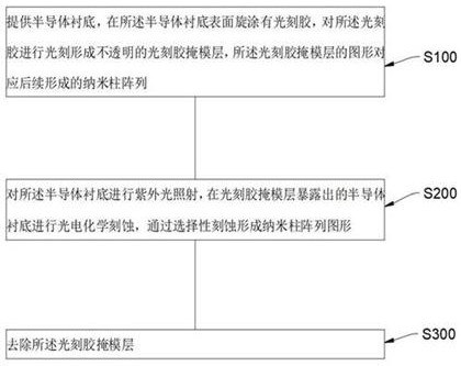
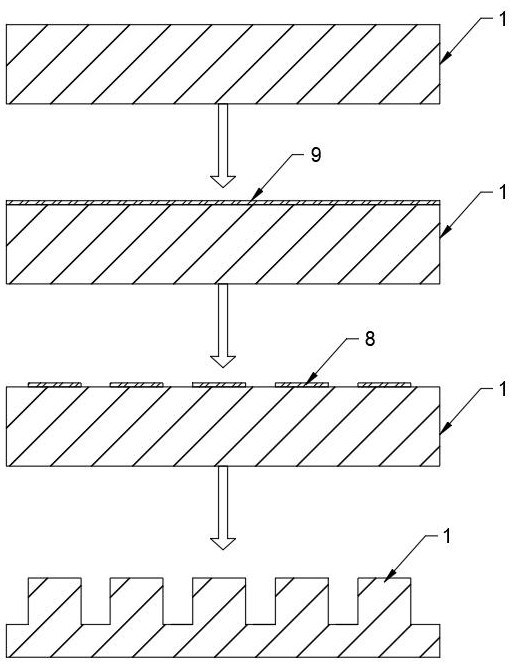
[0033] Such as figure 1 and figure 2 As shown, the embodiment of the present invention provides a method for preparing a nanopillar array, including:

[0034] In step S100, a semiconductor substrate is provided, and a photoresist is spin-coated on the surface of the semiconductor substrate, and photolithography is performed on the photoresist to form an opaque photoresist mask layer. The pattern of the photoresist mask layer corresponds to Subsequent formation of nanopillar arrays.

[0035] Step S200, irradiating the semiconductor substrate with ultraviolet light, performing photoelectrochemical etching on the semiconductor substrate exposed by the photoresist mask layer, and forming nano-column array patterns by selective etching.

[0036] Step S300, removing the photoresist mask layer.

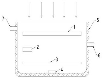
[0037] Specifically, step S100 is executed to provide a semiconductor substra...


PUM

PropertyMeasurementUnit
wavelengthaaaaaaaaaa
thicknessaaaaaaaaaa
diameteraaaaaaaaaa

Abstract

The invention relates to the field of process processing, in particular to a method for forming a nanopillar array on a semiconductor substrate, which comprises the following steps of: providing the semiconductor substrate, coating photoresist on the semiconductor substrate, and photoetching on the photoresist to form a pattern; a mask layer is formed on the prepared pattern, and light propagation is stopped through the mask layer; according to the method, a semiconductor substrate containing a mask layer is subjected to electrochemical etching, patterns with different heights are obtained by controlling etching conditions, then the mask layer is removed, the semiconductor substrate comprises a silicon carbide substrate slice or a gallium nitride substrate slice, the length and width of the semiconductor substrate are 2-8 inches, the thickness of the semiconductor substrate is 200-500 micrometers, and the thickness of the semiconductor substrate is 1-10 micrometers. An electron beam direct writing technology is adopted in the photoetching mode, and the pattern is in a nanopillar array shape. By adopting the photoelectrochemical etching method, the large-scale preparation of the nano-pillar array with controllable diameter size and height can be realized on the surface of the wafer-level wide bandgap semiconductor substrate slice, the process is simple, and the yield is high.

Description

technical field [0001] The invention relates to the field of semiconductor processing, in particular to a method for preparing a nanocolumn array. Background technique [0002] Wide bandgap semiconductor materials represented by gallium nitride, silicon carbide, zinc oxide and diamond have formed a global industrial chain of materials, devices and applications in the field of power semiconductors. The preparation of wide-bandgap semiconductor material nanowires or nanocolumns has increasingly become a research hotspot in the field of semiconductor devices, and has broad application prospects in nanoelectronics, superjunction power devices, lithium batteries and other new devices. [0003] With the continuous development of the manufacturing technology of the microelectronics industry, there are currently a variety of process methods to achieve specific applications in the field of micro-nano processing of nano-devices. At present, the preparation methods of nano-column struc...

Claims


Application Information

Patent Timeline
Patent Type & Authority Applications(China)
IPC IPC(8): H01L21/3063H01L21/308H01L21/04B82Y40/00
CPCH01L21/3081H01L21/30635H01L21/0475B82Y40/00
Inventor 皮孝东邵秦秦耿文浩王蓉杨德仁
Owner ZHEJIANG UNIV HANGZHOU GLOBAL SCI & TECH INNOVATION CENT
Why Eureka
Try Eureka