Electronic functional layer, preparation method of electronic functional layer and photoelectric device

A technology of functional layer and electron transport layer, which is applied in the direction of electric solid-state devices, electrical components, semiconductor devices, etc., can solve the problems of charge transport, poor injection efficiency, and affecting the luminous performance of devices, so as to improve electron transport efficiency and improve transport efficiency. Migration and injection efficiency, the effect of a wide range of activities

Pending Publication Date: 2022-05-13
TCL CORPORATION
View PDF0 Cites 0 Cited by
  • Summary
  • Abstract
  • Description
  • Claims
  • Application Information

AI Technical Summary

Problems solved by technology

[0004] The purpose of this application is to provide an electronic functional layer, a method for preparing an electronic functional layer, and a photoelectric device, aiming to solve the problem of poor charge transmission and injection efficiency in existing photoelectric devices such as QLEDs, which affects the performance of the device. Problems with luminous performance

Method used


Image

  • Electronic functional layer, preparation method of electronic functional layer and photoelectric device
  • Electronic functional layer, preparation method of electronic functional layer and photoelectric device
  • Electronic functional layer, preparation method of electronic functional layer and photoelectric device

Examples


preparation example Construction

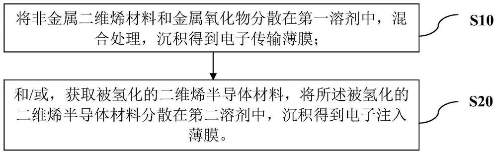
[0038] The second aspect of the embodiment of the present application provides a method for preparing an electronic functional layer, including steps:

[0039] S10. Dispersing the 2D semiconductor material and the electron transport material in the first solvent, mixing and processing, and depositing an electron transport film;

[0040] And / or, S20. Obtain the hydrogenated two-dimensional ene semiconductor material, disperse the hydrogenated two-dimensional ene semiconductor material in the second solvent, and deposit the electron injection film.

[0041] The preparation method of the electronic functional layer provided in the second aspect of the present application includes preparing an electron transport film doped with a two-dimensional ene semiconductor material, and / or preparing an electron injection film of a hydrogenated two-dimensional ene semiconductor material, the preparation method and process It is simple, can be flexibly adjusted according to actual application...

Embodiment 1

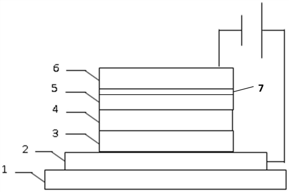
[0088] An electron transport material. In an argon atmosphere, silicene with a sheet diameter of 0.5-3 nm is nano-dispersed in n-octanol solvent. The concentration of silicene in the solution is 2 mg / mL. Ultrasonic waves can be used to accelerate its dispersion. After completely dissolving, put ZnO nanoparticles with a particle size of 2-5nm into the solution, the concentration of ZnO in the solvent is 10mg / mL, and stir at 25°C for 30min to obtain a silicene doping ratio of 1:5. The modified zinc oxide electron transport layer material solution is prepared for preparing QLED devices.

[0089] A QLED device, in which a hole injection layer, a hole transport layer, a quantum dot light-emitting layer, and an electron transport layer are spin-coated or deposited on an anode ITO substrate in sequence, and finally vapor-deposited on a cathode, and then packaged to form a QLED device. Wherein, what the quantum dots select is CdSeS / ZnS green quantum dots, what the hole transport layer...

Embodiment 2

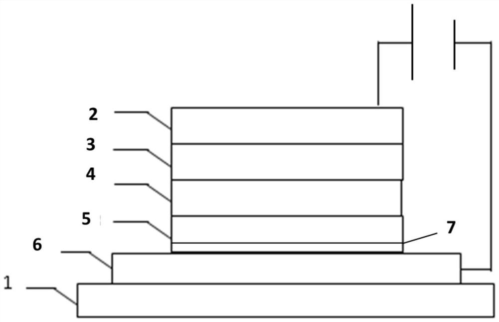
[0091] An electron transport material. In an argon atmosphere, germanene with a sheet diameter of 0.5-3nm is nano-dispersed in n-octanol solvent. The concentration of germanene in the solution is 2 mg / mL. Ultrasonic waves can be used to accelerate its dispersion. After complete dissolution, the TiO 2 nanoparticles into the solution, TiO 2 The concentration in the solvent was 20 mg / mL, and stirred at 20° C. for 30 min to prepare a modified titanium oxide electron transport layer material solution with a germanene doping ratio of 1:10, which was prepared for the preparation of QLED devices.

[0092] A QLED device, which differs from Example 1 mainly in that the germanene-modified titanium oxide electron transport layer material prepared in Example 2 is used for the electron transport layer.


PUM

PropertyMeasurementUnit
thicknessaaaaaaaaaa
thicknessaaaaaaaaaa
thicknessaaaaaaaaaa

Abstract

The invention belongs to the technical field of photoelectricity, and particularly relates to an electronic functional layer, a preparation method of the electronic functional layer and a photoelectric device. Wherein the electronic functional layer comprises a two-dimensional alkene semiconductor material. The two-dimensional alkene semiconductor material in the electronic functional layer has a honeycomb atomic structure, is rich in spin coupling orbits, is wide in activity range of electron cloud, is easy to radiate to similar particles to achieve a gain effect, and can effectively improve the electron transmission efficiency. When the compound is applied to a device, the luminous efficiency of a photoelectric device can be improved.

Description

technical field [0001] The application belongs to the field of photoelectric technology, and in particular relates to an electronic functional layer, a preparation method of the electronic functional layer, and a photoelectric device. Background technique [0002] Quantum dot light-emitting diode (QLED) has become a new generation of excellent display technology due to its advantages such as high luminous efficiency, high color purity, narrow luminous spectrum, and adjustable emission wavelength. Compared with OLED and traditional LCD, QLED has better competitive advantages in terms of color purity, color saturation and production cost. However, QLED still has problems such as low luminous efficiency, low lifespan, and poor stability, which limit the large-scale commercial application of QLED. [0003] At present, the main reason for the low luminous efficiency and low lifespan of QLEDs is that the hole-electron transfer efficiency in QLED devices is not high, which leads t...

Claims


Application Information

Patent Timeline
Patent Type & Authority Applications(China)
IPC IPC(8): H01L51/50H01L51/54H01L51/56
CPCH10K50/115H10K50/16H10K50/171H10K2102/00H10K71/00
Inventor 吴劲衡吴龙佳何斯纳
Owner TCL CORPORATION
Why Eureka
Try Eureka