Silicon carbide MOSFET device and preparation method thereof

A technology of silicon carbide and silicon carbide substrates, applied in semiconductor/solid-state device manufacturing, semiconductor devices, electrical components, etc., to achieve high channel carrier mobility, improve channel current capability, and reduce JFET area resistance Effect

Pending Publication Date: 2022-06-10
ZHUZHOU CRRC TIMES SEMICON CO LTD
View PDF2 Cites 0 Cited by
  • Summary
  • Abstract
  • Description
  • Claims
  • Application Information

AI Technical Summary

Problems solved by technology

Chinese patent CN201110171696.0 discloses a SiC IEMOSFET device with an epitaxial channel and its manufacturing method. The conductive channel in the working state is far away from the SiO2 and SiC interface, reducing the impact of surface scattering on electron mobility. In order to solve the problems of low channel electron mobility and large conductor resistance of existing SiC IEMOSFET devices
However, the methods provided by these two patents increase the channel leakage when the device is reversed, and the inversion of the N-type film when the device is turned off prolongs the turn-off time of the device

Method used


Image

  • Silicon carbide MOSFET device and preparation method thereof
  • Silicon carbide MOSFET device and preparation method thereof
  • Silicon carbide MOSFET device and preparation method thereof

Examples


Embodiment Construction

[0039] Below in conjunction with accompanying drawing and specific embodiment, technical solution of the present invention is described further in detail:

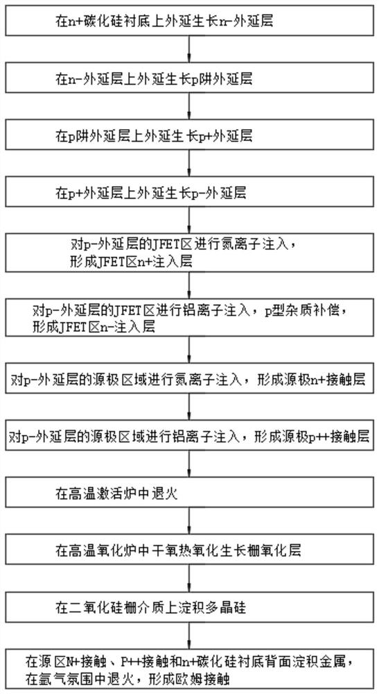
[0040] Please also refer to Figure 2-Figure 3k , the preparation method of the silicon carbide MOSFET device provided in this embodiment, comprises the following steps:

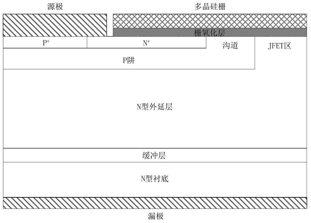
[0042] Step 1, epitaxial growth on n+ silicon carbide substrate with a doping concentration of 1e15cm -3 ~9e15cm -3 , an n-epitaxial layer with a thickness of 8-50 μm; as Figure 3a shown;

[0043] Step 2, epitaxial growth on the n- epitaxial layer with a doping concentration of 4e16cm -3 ~8e16cm -3 , a p-well epitaxial layer with a thickness of 0.5-0.7 μm; such as Figure 3b shown;

[0044] Step 3, epitaxial growth on the p-well epitaxial layer with a doping concentration of 3e18cm -3 ~7e18cm -3 , a p+ epitaxial layer with a thickness of 0.3-0.4 μm; such as Figure 3c shown;

[0045] Step 4, epitaxial growth on the p+ epitaxial layer with a...


PUM

PropertyMeasurementUnit
thicknessaaaaaaaaaa
thicknessaaaaaaaaaa
thicknessaaaaaaaaaa

Abstract

The invention provides a preparation method of a silicon carbide MOSFET (Metal-Oxide-Semiconductor Field Effect Transistor) device. The preparation method comprises the following steps: step 1, growing an n-epitaxial layer on an n + silicon carbide substrate; 2, growing a p well epitaxial layer; step 3, growing a p + epitaxial layer; step 4, growing a p-epitaxial layer; step 5, forming a JFET region n + injection layer; step 6, forming a JFET region n-injection layer; step 7, forming a source electrode n + contact layer; step 8, forming a source p + + contact layer; step 9, annealing in a high-temperature activation furnace; step 10, growing a gate oxide layer in a high-temperature oxidation furnace through dry-oxygen thermal oxidation; step 11, depositing polycrystalline silicon on the silicon dioxide gate dielectric to form a gate electrode; 12, metal is deposited on the N + contact, the P + + contact and the back face of the n + silicon carbide substrate in the source region, ohmic contact is formed after annealing, and a source electrode and a drain electrode are formed; according to the preparation method of the silicon carbide MOSFET device provided by the invention, the negative influence of channel electron mobility reduction caused by injection can be reduced, the on-resistance of the device is reduced, and the current output capability is improved.

Description

technical field [0001] The invention belongs to the field of semiconductor device manufacturing, and in particular relates to a silicon carbide MOSFET device and a preparation method thereof. Background technique [0002] Silicon carbide (SiC), as the third-generation wide-bandgap semiconductor material, has excellent characteristics such as high electron saturation velocity, high voltage resistance, radiation resistance, and high temperature resistance. As the only one capable of direct thermal oxidation to form SiO 2 The wide bandgap semiconductor material of the gate insulating layer, SiC-based MOSFET devices have been widely used in many fields such as switching power supplies, high-frequency heating, electric vehicles, and power amplifiers. [0003] Traditional SiC MOSFET structures such as figure 1 As shown, the P well is usually realized by ion implantation, and the implanted ions are activated by high temperature activation annealing. Since high-temperature anneal...

Claims


Application Information

Patent Timeline
Patent Type & Authority Applications(China)
IPC IPC(8): H01L21/336H01L29/10H01L29/78
CPCH01L29/66068H01L29/1033H01L29/7827
Inventor 李诚瞻罗烨辉郑昌伟赵艳黎刘芹戴小平
Owner ZHUZHOU CRRC TIMES SEMICON CO LTD
Why Eureka
Try Eureka