Preparation method of electron transport layer and light emitting diode
A technology of electron transport layer and light-emitting diode, which is applied in the direction of circuits, electrical components, electric solid devices, etc., can solve the problem of single material selection, achieve good light transmission, high conductivity, and facilitate the effect of charge transport concentration
- Summary
- Abstract
- Description
- Claims
- Application Information
AI Technical Summary
Problems solved by technology
Method used
Image

Examples
preparation example Construction
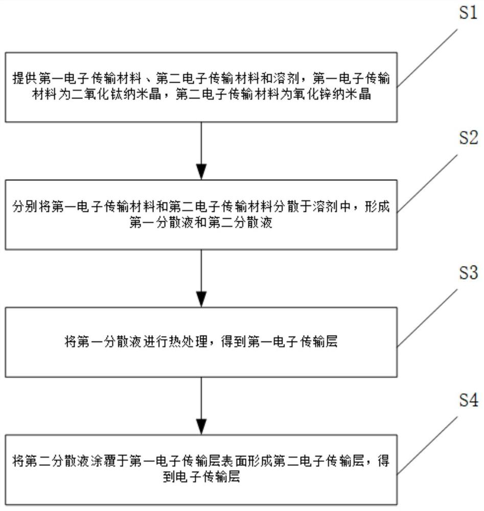
[0039] like figure 1 As shown, an embodiment of the present invention provides a method for preparing an electron transport layer, which includes the following steps:
[0040] S1, providing a first electron transport material, a second electron transport material and a solvent, the first electron transport material is titanium dioxide nanocrystals, and the second electron transport material is zinc oxide nanocrystals;
[0041] S2, respectively dispersing the first electron transport material and the second electron transport material in a solvent to form a first dispersion liquid and a second dispersion liquid;
[0042] S3, heat-treating the first dispersion to obtain a first electron transport layer;
[0043] S4, coating the second dispersion liquid on the surface of the first electron transport layer to form a second electron transport layer to obtain an electron transport layer.
[0044] Titanium dioxide nanocrystals are a wide-bandgap inorganic semiconductor material with ...
Embodiment 1
[0092] This embodiment provides a method for preparing an electron transport layer of a quantum dot light-emitting diode, comprising the following steps:
[0093] (31) Mix 1.4ml TX-100 with 7.6ml absolute ethanol, add 24mmol acetic acid and 24mmol tetraisopropyl titanate, stir vigorously for 10min at room temperature to obtain TiO 2 Precursor solution, using absolute ethanol to convert TiO 2 The precursor solution was diluted 10 times, placed in the air, and continued to stir for 30 min to slowly grow to obtain a titanium dioxide nanocrystal solution with an average particle size of 9 nm and a concentration of 20 mg / mL;
[0094] (32) spin-coating the titania nanocrystal solution obtained in step (31) on a clean IZO glass substrate, and placing it in a tube furnace with a hydrogen pressure of 1.5 MPa and a temperature of 500° C. for 30 min to obtain a first surface with oxygen-rich vacancies on the surface. an electron transport layer with a thickness of 18 nm;
[0095] (33) ...
Embodiment 2
[0097]This embodiment provides a method for preparing an electron transport layer of a quantum dot light-emitting diode, comprising the following steps:
[0098] (41) Mix 1.4ml of nonylphenol polyoxyethylene ether with 7.6ml of absolute ethanol, add 24mmol of acetic acid and 24mmol of tetraisopropyl titanate, stir vigorously for 10min at room temperature to obtain TiO 2 Precursor solution, using absolute ethanol to convert TiO 2 The precursor solution was diluted 20 times, placed in the air, and continued to stir for 30 min to slowly grow to obtain a titanium dioxide nanocrystal solution with an average particle size of 11 nm and a concentration of 10 mg / mL;
[0099] (42) spin-coating the titanium dioxide nanocrystal solution obtained in step (41) on a clean IZO glass substrate, placing it in a tube furnace with a hydrogen pressure of 2 MPa and a temperature of 450° C. for 30 min to obtain the first surface oxygen-rich vacancy An electron transport layer with a thickness of 1...
PUM
| Property | Measurement | Unit |
|---|---|---|
| Thickness | aaaaa | aaaaa |
| Thickness | aaaaa | aaaaa |
| The average particle size | aaaaa | aaaaa |
Abstract
Description
Claims
Application Information
 - R&D
- Intellectual Property
- Life Sciences
- Materials
- Tech Scout
- Unparalleled Data Quality
- Higher Quality Content
- 60% Fewer Hallucinations
Browse by: Latest US Patents, China's latest patents, Technical Efficacy Thesaurus, Application Domain, Technology Topic, Popular Technical Reports.
© 2025 PatSnap. All rights reserved.Legal|Privacy policy|Modern Slavery Act Transparency Statement|Sitemap|About US| Contact US: help@patsnap.com