

Preparation method and application of film with photonic device structure
A technology of photonic devices and thin films, applied in optical components, coupling of optical waveguides, instruments, etc., can solve problems such as high cost, limited application, complicated process, etc., and achieve the effects of low optical loss, fast response, and simple processing technology
- Summary
- Abstract
- Description
- Claims
- Application Information
AI Technical Summary
Problems solved by technology
Method used
Image

Examples
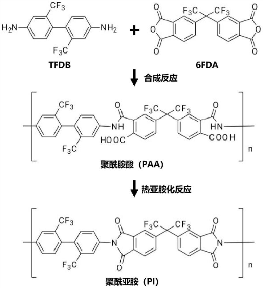
Embodiment 1
[0055] Synthesis of polyamic acid:
[0056] (1) in the three-necked flask, add anhydrous solvent DMAC 50mL, then weigh 5g of TFDB and add the solvent, under nitrogen protection, mechanically stir at a speed of 100 rev / min until dissolved to obtain a colorless transparent solution;
[0057] (2) Weigh 6FDA 6.93g, add the transparent solution of TFDB in 5 times, after the last addition in the process, under nitrogen protection, mechanically stir at a speed of 100 rpm until the dissolution is complete, and then repeat the operation to carry out the following Join at a time until all joins are completed at the end;
[0058] (3) after the addition of (2) is completed, after the solution is clarified, the rotating speed is increased to 300 rpm, and at 25 ° C, the reaction is performed for 22 hours, and finally PAA (polyamic acid) is obtained;
[0059] (4) Transfer the PAA into a clean glass bottle and store in a refrigerator at 5°C for later use.
[0060] Preparation of polyimide f...
PUM
| Property | Measurement | Unit |
|---|---|---|
| diameter | aaaaa | aaaaa |
Abstract
Description
Claims
Application Information