Multi-quantum well-based light emitting diode and preparation method thereof
A technology for light-emitting diodes and multiple quantum wells, which is applied to semiconductor devices, electrical components, circuits, etc., can solve problems such as affecting the luminous efficiency of multiple quantum well-based light-emitting diodes, reducing the crystal quality of multiple quantum well layers, and improving atomic mobility. , the effect of improving crystal quality and improving efficiency
- Summary
- Abstract
- Description
- Claims
- Application Information
AI Technical Summary
Problems solved by technology
Method used
Image

Examples
Embodiment 1
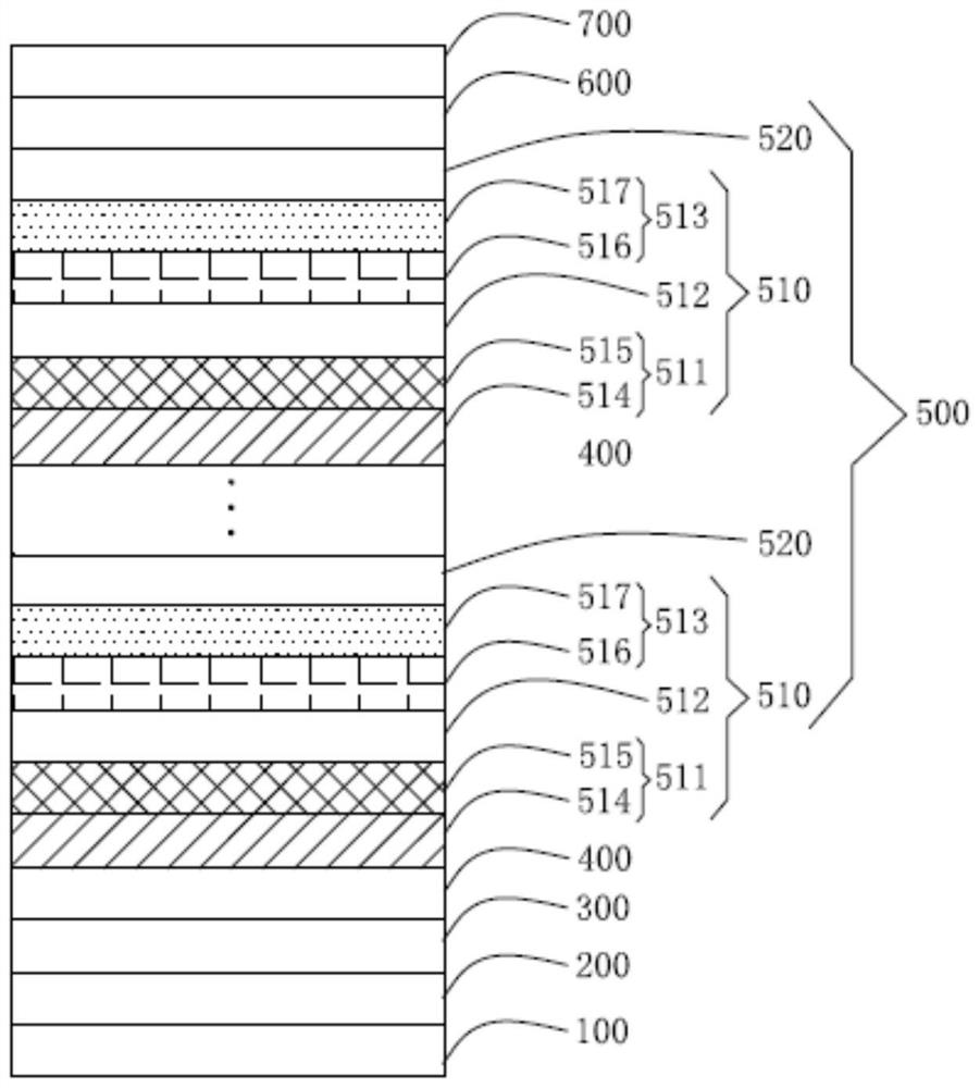
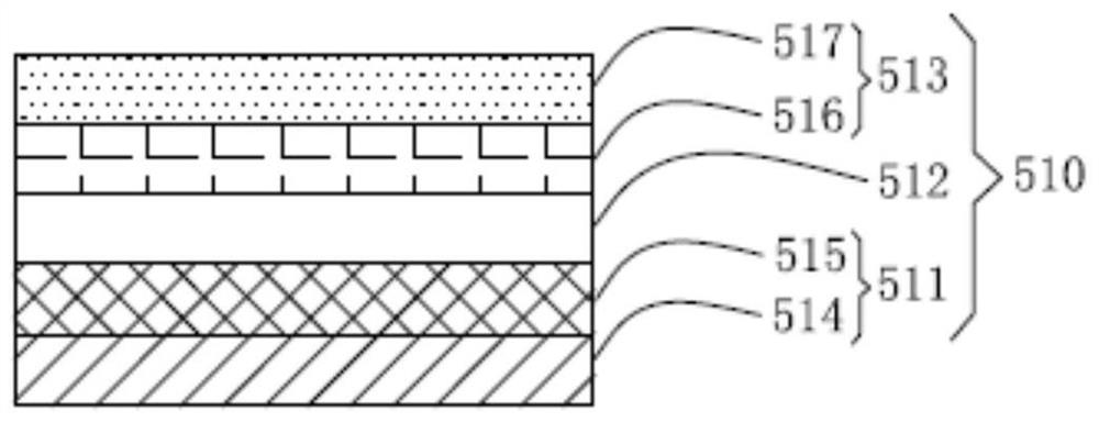
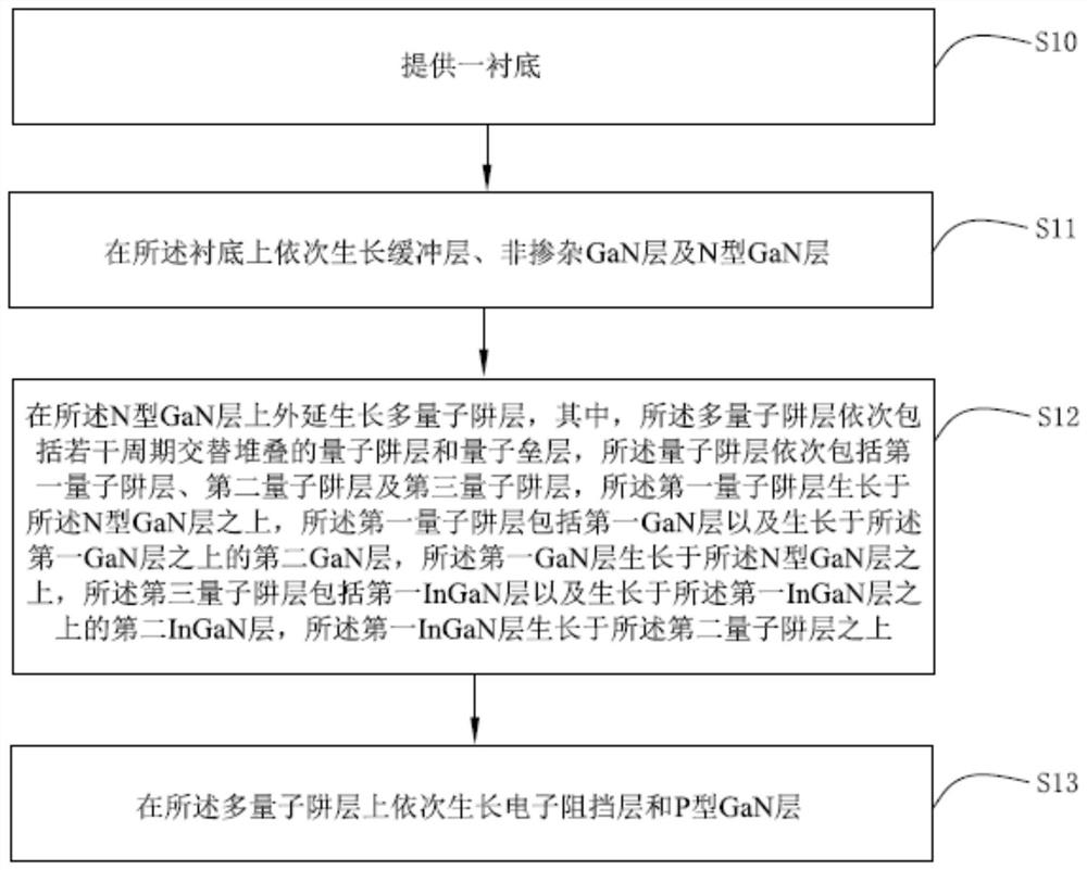
[0038] see Figure 1-Figure 2 , shows a multi-quantum well-based light-emitting diode provided by the first embodiment of the present invention, the multi-quantum well-based light-emitting diode includes a substrate 100; wherein, the substrate 100 is a substrate for epitaxial layer growth, and the commonly used substrate 100 For sapphire substrate, SiO 2 Sapphire composite substrate, silicon substrate, silicon carbide substrate, gallium nitride substrate and zinc oxide substrate, in this embodiment, the material of the substrate 100 is sapphire, and sapphire has good light transmittance, high temperature resistance and corrosion resistance , The advantages of mature preparation process and low price, etc., are widely used in multi-quantum well-based light-emitting diodes.
[0039] A buffer layer 200, an undoped GaN layer 300, an N-type GaN layer 400, a multiple quantum well layer 500, an electron blocking layer 600 and a P-type GaN layer 700 are sequentially stacked on the su...
Embodiment 2
[0056] The second embodiment of the present invention provides a multi-quantum well-based light-emitting diode. The multi-quantum well-based light-emitting diode in this embodiment is different from the multi-quantum well-based light-emitting diode in the first embodiment in that:
[0057] The thickness of the quantum well layer is 3.2 nm. Other conditions are the same. The thickness ratio of the first GaN layer, the second GaN layer, the second quantum well sublayer, the first InGaN layer and the second InGaN layer is 1.5:1:1 : 4:1, the In composition of the second quantum well sublayer is graded from low to high from 0.05 to 0.25, the In composition of the first InGaN layer is 0.25, the In composition of the second InGaN layer is 0.25, the first GaN The growth temperature of the layer is 850°C, the growth temperature of the second GaN layer is decreased from 850°C to 810°C, and the growth is performed while decreasing, and the growth temperature of the second quantum well sub...
Embodiment 3
[0059] The third embodiment of the present invention provides a multi-quantum well-based light-emitting diode. The multi-quantum well-based light-emitting diode in this embodiment is different from the multi-quantum well-based light-emitting diode in the first embodiment in that:
[0060] The thickness of the quantum well layer is 3.7 nm. Other conditions are the same. The thickness ratio of the first GaN layer, the second GaN layer, the second quantum well sublayer, the first InGaN layer and the second InGaN layer is 1.5:1:1 : 4:1, the In composition of the second quantum well sublayer is graded from low to high from 0.05 to 0.25, the In composition of the first InGaN layer is 0.25, the In composition of the second InGaN layer is 0.25, the first GaN The growth temperature of the layer is 850°C, the growth temperature of the second GaN layer is decreased from 850°C to 810°C, and the growth is performed while decreasing, and the growth temperature of the second quantum well sub-...
PUM
| Property | Measurement | Unit |
|---|---|---|
| thickness | aaaaa | aaaaa |
| thickness | aaaaa | aaaaa |
| thickness | aaaaa | aaaaa |
Abstract
Description
Claims
Application Information
 - R&D
- Intellectual Property
- Life Sciences
- Materials
- Tech Scout
- Unparalleled Data Quality
- Higher Quality Content
- 60% Fewer Hallucinations
Browse by: Latest US Patents, China's latest patents, Technical Efficacy Thesaurus, Application Domain, Technology Topic, Popular Technical Reports.
© 2025 PatSnap. All rights reserved.Legal|Privacy policy|Modern Slavery Act Transparency Statement|Sitemap|About US| Contact US: help@patsnap.com