Device and method for cleaning semiconductor wafer after wet etching of oxide layer

A wet etching and semiconductor technology, applied in the field of microelectronics, can solve problems such as low flow speed, reduced operating efficiency, particle pollution, etc., and achieve the effect of enhancing the scouring ability and increasing the scouring effect

Pending Publication Date: 2022-08-05
湖南杰楚微半导体科技有限公司
View PDF0 Cites 0 Cited by
  • Summary
  • Abstract
  • Description
  • Claims
  • Application Information

AI Technical Summary

Problems solved by technology

[0005] In order to solve the problem of chemical residue and particle contamination after wet etching, the existing traditional method mainly uses the overflow cleaning method, immersing the semiconductor wafer in the cleaning tank, and then water overflows from the top of the cleaning tank to complete the cleaning of the semiconductor wafer. The overflow cleaning of the wafer has the following defects: (1) the lack of chemical cleaning ability, this is because the water flow of the overflow cleaning is injected into the tank from the bottom, and the cross-sectional area of ​​the tank is very wide, and the water flows in the tank. The flow velocity of the body from bottom to top is very low, so the flushing ability is poor; (2) the ability to remove particles is poor. After entering the cleaning tank, the semiconductor wafer is completely submerged in water, but from a microscopic point of view, it has adhered The local interface of the particle is water-repellent because of the large approach angle of the wafer surface, so that water cannot enter the interface between the particle and the wafer, and it is difficult to cut the bottom of the particle. Pressed on the surface of the wafer, it is more difficult to be removed; (3) Large flow and long flushing time are required to achieve the necessary cleanliness, which brings greater consumption of ultrapure water and longer working time, pushing up Reduce cleaning costs and reduce operating efficiency

Method used


Image

  • Device and method for cleaning semiconductor wafer after wet etching of oxide layer
  • Device and method for cleaning semiconductor wafer after wet etching of oxide layer
  • Device and method for cleaning semiconductor wafer after wet etching of oxide layer

Examples


Embodiment 1

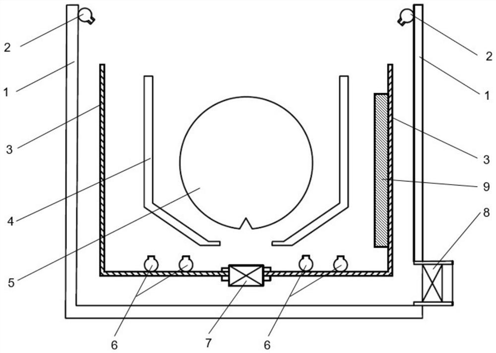
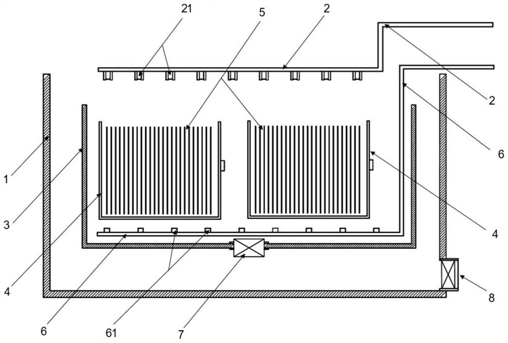
[0037] like figure 1 and figure 2 It is shown that the embodiment is used to clean the device of the semiconductor wafer of the rear semiconductor wafer of the wetting method of the wetting method, including outer slot 1, the inner slot 3 inside the outer slot 1, and the inner slot 3 is used to place it to clean the semiconductor crystal crystal The round Jingzhou 4, the top cloth of Jingzhou 4 is equipped with two spray water pipes 2 for spraying to clean the semiconductor wafer, and the spray water pipe 2 is installed on the left and right sides of the long side of the outer groove 1, which is higher than the height than Inner groove 3 overall height; the bottom of the inner slot 3 is provided with several water supply pipes 6 and the first fast drainage valve 7. In the present invention, the number of spray water pipe 2 and its diameter can be adjusted regularly according to actual needs.

[0038] In the present invention, the inner slot is set in the outer groove, and the spra...

Embodiment 2

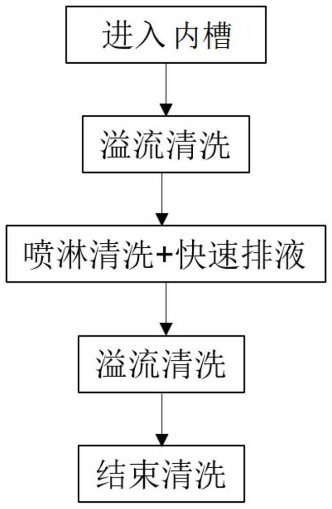
[0045] A method for cleaning the wet etching oxide layer's rear semiconductor wafer, specifically the device used in an embodiment 1 for cleaning the wet etching oxidation layer's rear semiconductor wafer Cleaning treatment of the rear semiconductor wafer) of the oxygen layer, the schematic diagram of the cleaning process is image 3 It includes the following steps:

[0046] S1. Place semiconductor wafer 5 after the completion of the wet etching oxide layer is placed in Jingzhou 4, put it into the inner slot 3, open the first fast drain valve 7, and open the spray water pipe 2 at the same time. Under the condition of 40L / min, the washing semiconductor wafer was scrubbed at 150s. In this step, in the traditional cleaning scheme, due to the adsorption of chemicals, and the pellets due to the pressure of the wafer surface, the particles are only under the pressure of the water pressure and have no internal cutting effect. The cleaning effect of the particles is not ideal. Based on thi...


PUM

PropertyMeasurementUnit
pore sizeaaaaaaaaaa
pore sizeaaaaaaaaaa

Abstract

The invention discloses a device and a method for cleaning a semiconductor wafer after wet etching of an oxide layer, the device comprises an outer groove, an inner groove and a wafer boat for placing the semiconductor wafer to be cleaned are arranged in the outer groove in sequence, a plurality of spraying water pipes for spraying the semiconductor wafer to be cleaned are arranged above the wafer boat, and the spraying water pipes are communicated with the inner groove. A plurality of water supply pipes and a first quick drain valve are arranged at the bottom of the inner tank. According to the cleaning method, the device is adopted for cleaning treatment. Compared with a conventional cleaning device, the cleaning device has the advantages that the capability of removing residual chemicals is enhanced, and the capability of removing particles on the surface of the wafer is also enhanced, so that particle pollutants and residual chemicals on the surface of the wafer can be effectively removed, the use value is high, and the application prospect is good. The cleaning method has the advantages of being convenient to operate, low in processing cost, high in processing efficiency, good in cleaning effect and the like, efficient cleaning of the surface of the semiconductor wafer can be achieved, and the cleaning method has great significance in promoting wide application of the semiconductor wafer.

Description

Technical field [0001] The invention belongs to the field of microelectronics, involving a cleaning device and cleaning method of a semiconductor wafer, which specifically involves a device and method and method for cleaning the semiconductor wafers of the rear semiconductor wafer of the wet oxide layer. Background technique [0002] The semiconductor industry is often used as a medium layer. It has an insulation that can block the current. It can also form a capacitor as a medium isolation layer, and it can also be used as a cover material to protect the substrate for plasma etching or ion injection. The silicon oxide can be obtained on the single crystal silicon substrate, and it can also be obtained through the deposition of chemical gas. It is small with the lattice of the silicon substrate, the thermal expansion coefficient is close, and the internal stress is small. It is a common material for semiconductor. [0003] The etching of silicon oxide can be carved by plasma ecli...

Claims


Application Information

Patent Timeline
Patent Type & Authority Applications(China)
IPC IPC(8): H01L21/67H01L21/02B08B3/02
CPCH01L21/67051H01L21/0206B08B3/02Y02P70/50
Inventor 陈章隆石福荣尹凌云马玉玺易文杰吕文利谢于柳
Owner 湖南杰楚微半导体科技有限公司
Why Eureka
Try Eureka