Eureka AIR delivers breakthrough ideas for toughest innovation challenges, trusted by R&D personnel around the world.

Silicon-based gallium nitride epitaxial wafer and manufacturing method thereof

A manufacturing method and epitaxial wafer technology, applied in the direction of final product manufacturing, sustainable manufacturing/processing, climate sustainability, etc., can solve the problem of high dislocation density in GaN epitaxy, and achieve good stress transfer and coordinated release effects , reduce thermal mismatch, reduce the effect of lattice mismatch and thermal mismatch

Pending Publication Date: 2022-08-05
JIANGXI ZHAO CHI SEMICON CO LTD
View PDF0 Cites 5 Cited by
  • Summary
  • Abstract
  • Description
  • Claims
  • Application Information

AI Technical Summary

Problems solved by technology

[0005] Based on this, the object of the present invention is to provide a silicon-based gallium nitride epitaxial wafer and its manufacturing method, so as to fundamentally solve the problem of high dislocation density of the existing gallium nitride epitaxy using a silicon substrate

Method used


Image

  • Silicon-based gallium nitride epitaxial wafer and manufacturing method thereof
  • Silicon-based gallium nitride epitaxial wafer and manufacturing method thereof
  • Silicon-based gallium nitride epitaxial wafer and manufacturing method thereof

Examples


Embodiment 1

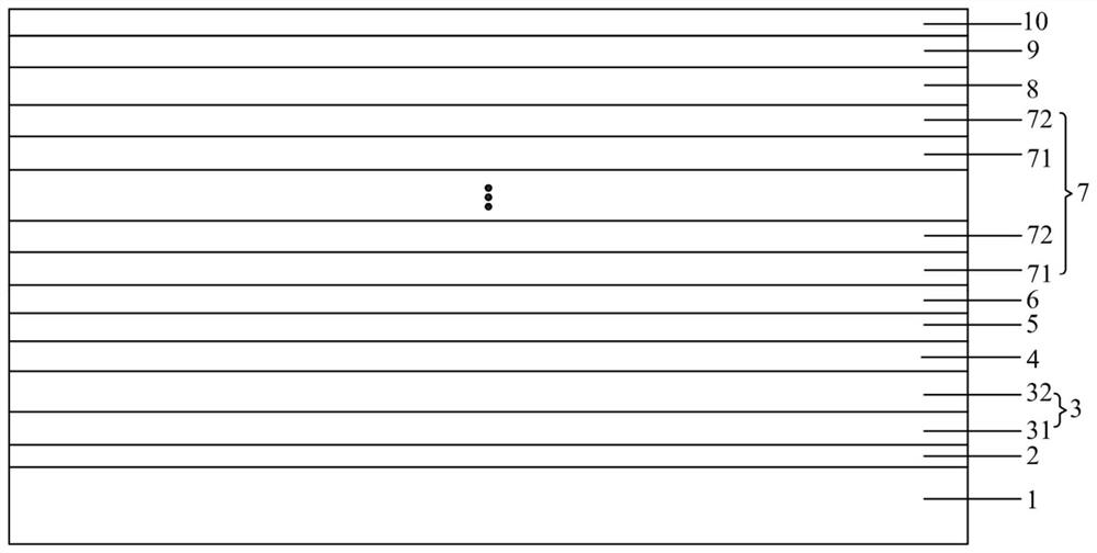
[0048] See figure 1 It is a structural diagram of a silicon -based nitrogen nitrogen -nitride extension of the embodiments of the present invention. In order to facilitate the explanation, only parts related to the embodiments of the invention are displayed. The film includes:

[0049] Silicon lining 1. AL layer on the silicon substrate 1 in sequence 2. ALN formation of nuclear layer 3. Stress variable layer 4. N. N, bits and fine -tuning layers 6, multi -quantum trap layer 7, electronic blocking layer, electronic blocking layer 8. P -shaped layer 9 and P type contact layer 10;

[0050] Aln formation nuclear layer 3 includes Aln three -dimensional nuclear layer 31 and ALN two -dimensional nuclear layer 32;

[0051] Stress Merrage 4 is Al x B y GA 1-x-y N layer, of which 0

[0052] The fine -tuning layer 6 is any or more combination of Aln layer, BN layer, and Bgan layer.

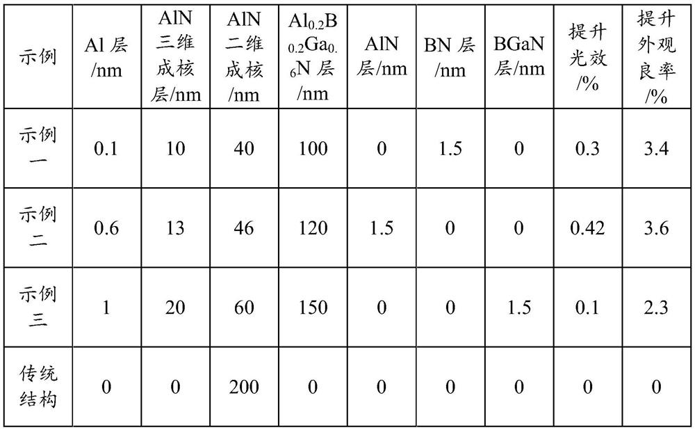
[0053] Among them, in one embodiment of the present invention, it uses silicon substrate ...

Embodiment 2

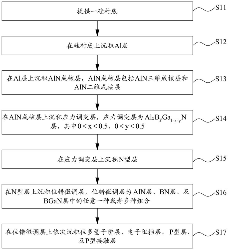
[0068] See figure 2 It is a silicon -based nitrogen -nitride extension chip preparation method in the second embodiment of the present invention, which specifically includes step S11 to step S17.

[0069] Step s1, provide a silicon substrate.

[0070] Among them, in the embodiments of the present invention, the specific use of silicon substrate is used as the extension of the substrate, and it can be graphical silicon substrate or flat silicon lining when used. Further, the present invention uses metal organic chemical gas deposition (MOCVD) equipment to grow extension. Among them, high -purity ammonia (NH 3 ) As a source of N (nitrogen), the three -based base (TMGA) as the source of GA (镓), the three -based 铟 (TMIN) is in (铟) source, and the triangular aluminum (TMAL) is used as Al (aluminum) source, Boron chloride (BCL 3 ) As a source of B (boron), the Sih (SIH 4 ) As a N -type dopant, Er Mao Magnesium (CP 2 Mg) as a P -type dopant. By adopting high -pure H 2 (Hydrogen) or n 2 (...


PUM

PropertyMeasurementUnit
thicknessaaaaaaaaaa
thicknessaaaaaaaaaa
thicknessaaaaaaaaaa

Abstract

The invention provides a silicon-based gallium nitride epitaxial wafer and a manufacturing method thereof. The silicon-based gallium nitride epitaxial wafer comprises a silicon substrate, an Al layer, an AlN nucleating layer, a stress modulation layer, an N-type layer, a dislocation fine tuning layer, a multi-quantum well layer, an electron blocking layer, a P-type layer and a P-type contact layer, the AlN nucleating layer comprises an AlN three-dimensional nucleating layer and an AlN two-dimensional nucleating layer; the stress modulation layer is an Al < x > B < y > Ga < 1-x-y > N layer, x is more than 0 and less than 0.5, and y is more than 0 and less than 0.5; the dislocation fine tuning layer is any one or a combination of more of an AlN layer, a BN layer and a BGaN layer. According to the invention, the problem of large dislocation density of the existing gallium nitride epitaxy adopting the silicon substrate is solved.

Description

Technical field [0001] The invention involves the field of photoelectric technology, and specially involves a silicon -based nitrogen -nitrogen extension and its production method. Background technique [0002] The research and application of the III nitride -nitride semiconductor material is a hot topic in the semiconductor industry. As the representative of the Ⅲ nitrogen -nitride semiconductor material, GAN (nitride) has developed greatly in the fields of light emitting diode and high -power electronic devices due to its excellent electronics and optical properties. [0003] Because GAN single crystals are still in the experimental stage, the heterogeneous extension of GAN materials is inevitable. The substrate materials include sapphire, SIC (silicon carbide), and SI (silicon) substrates. Compared with sapphire and SIC, the SI substrate has the advantages of low price, high quality, high thermal conductivity, good conductivity, and maturity of large diameter single crystal gr...

Claims


Application Information

Patent Timeline
Patent Type & Authority Applications(China)
IPC IPC(8): H01L33/12H01L33/16H01L33/32H01L33/00H01L33/06
CPCH01L33/12H01L33/16H01L33/06H01L33/325H01L33/007Y02P70/50
Inventor 郑文杰程龙高虹曾家明刘春杨胡加辉
Owner JIANGXI ZHAO CHI SEMICON CO LTD
Why Eureka
Eureka Blog
Learn More