Integration of continuous self-aligning semiconductor photoelectronic device and mode spot converter

A technology for optoelectronic devices and mode-spot converters, which is used in semiconductor lasers, semiconductor/solid-state device manufacturing, laser parts and other directions, and can solve problems such as large strain differences, difficulty in obtaining high-quality materials, and high crystal quality.

Inactive Publication Date: 2006-01-25
INST OF SEMICONDUCTORS - CHINESE ACAD OF SCI
View PDF0 Cites 0 Cited by
  • Summary
  • Abstract
  • Description
  • Claims
  • Application Information

AI Technical Summary

Problems solved by technology

In the mode spot converter with gradually narrowed transverse waveguide width, etching technology is used to form lateral wedges. In order to make the mode conversion efficiency high, the etched strip width must be 2 ) coverage, and only select one side of the growing speckle converter; but because the length of the speckle converter is usually shorter, and the optoelectronic device integrated with it is longer, in this way, most of the speckle converter grows as SiO 2 Coverage greatly affects the quality of selected growth materials, especially in the docking part of the two devices, it is difficult to obtain high-quality materials, which greatly affects the coupling efficiency of the two devices and the overall output power of the device
Moreover, it is very difficult to fully realize the connection between the mode spot converter and the active region of the optoelectronic device.
(2) When selecting the growth mode spot converter (SSC), do not use SiO on the side of the optoelectronic device 2 However, it is grown at the same time and used as the upper waveguide layer of the optoelectronic device, which realizes the self-aligned docking between the optoelectronic device and the SSC, but due to the thickness modulation effect and strain modulation in the selective growth process effect, due to the absence of SiO on the side of the optoelectronic device 2 covered, and the SiO on both sides of the SSC connected with it 2 The width is the widest, so the strain difference between the optoelectronic device and the SSC is the largest, and it is difficult to obtain high crystal quality at the joint between the two

Method used


Image

  • Integration of continuous self-aligning semiconductor photoelectronic device and mode spot converter
  • Integration of continuous self-aligning semiconductor photoelectronic device and mode spot converter
  • Integration of continuous self-aligning semiconductor photoelectronic device and mode spot converter

Examples


Embodiment 1

[0032] Example 1: Integration of polarization insensitive semiconductor optical amplifier SOA+SSC

[0033] The polarization insensitive semiconductor optical amplifier prepared by the present invention is integrated with the SSC, and the preparation steps include the following:

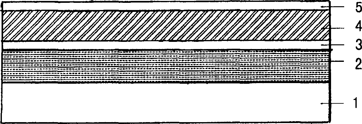
[0034] 1) Use metal organic chemical vapor deposition (MOCVD) to sequentially grow InP buffer layer, InGaAsP (InGaAsP) lower waveguide layer, InP isolation layer, SOA active area, and InP on an n-type indium phosphorus (InP) substrate. Protective layer (e.g. figure 1 Shown);

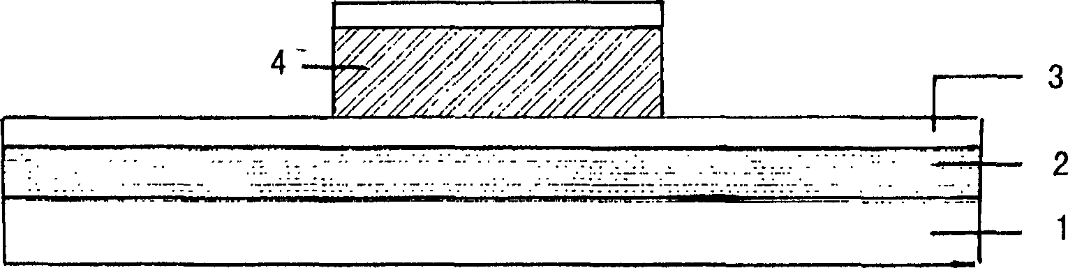
[0035] 2) Use ordinary photolithography etching technology to photoetch the SSC area to the InP isolation layer, such as figure 2 Shown

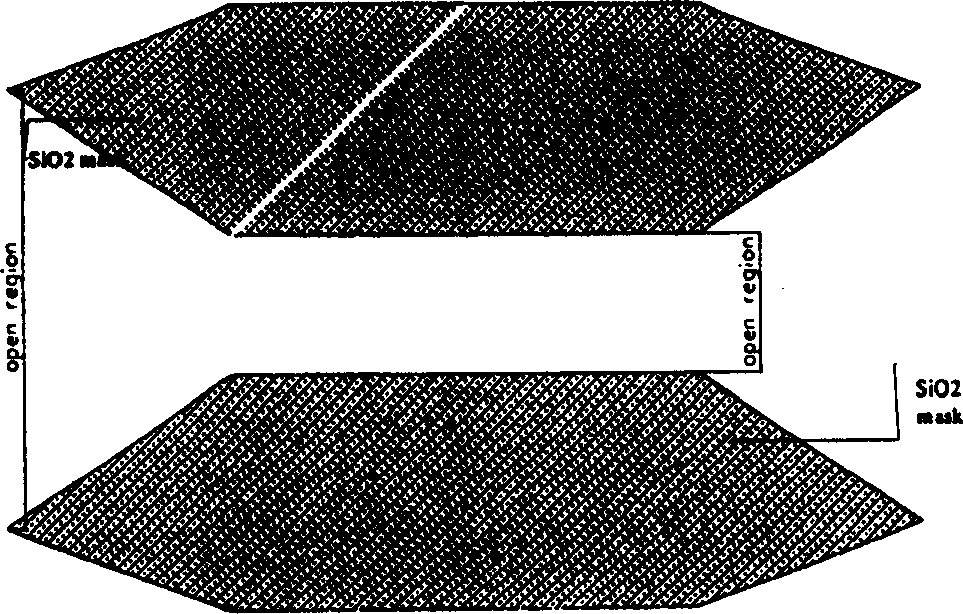
[0036] 3) Using plasma chemical deposition technology to grow SiO 2 150nm;

[0037] 4) Use as image 3 Lithography etched out Figure 4 Graphics

[0038] 5) Use hydrochloric acid to etch away the InP protection layer in the SOA part and the indium phosphorus isolation layer in the SSC area;

[0...

Embodiment 2

[0048] Embodiment 2: Integration of electro-absorption modulator and SSC

[0049] This kind of device is exactly the same as Special Case 1 in the electro-absorption modulator and SSC integration part, but in the subsequent process, according to the characteristics of the electro-absorption modulator, a ridge waveguide structure needs to be used and the production of electrodes needs to be filled with a low-dielectric constant dielectric substance. And the use of pattern electrodes.

Embodiment 3

[0050] Embodiment 3: Integration of Distributed Feedback Laser (DFB) and SSC:

[0051] This kind of device is almost the same in the integration part of DFB and SSC as Special Case 1, but because DFB is a light-emitting device, it only needs to be integrated with SSC at a single end. After completing the selective growth SSC part, the following preparation steps must be adopted:

[0052]1) The protective layer InGaAsP and the cap layer InP are sequentially etched away with a selective etching solution;

[0053] 2) Make a grating in the DFB part, as shown in Figure 6(a);

[0054] 3) P-InP cap layer and InGaAsP protective layer are grown on the grating and SSC, as shown in Figure 6(b);

[0055] 4) After that, the BH strip waveguide structure is prepared in the same way as in Special Example 1.

[0056] 5) According to the high frequency characteristics, pattern electrodes should be made on the DFB side;

[0057] 6) Plating high reflection film on one end of DFB and antireflection fi...


PUM


Abstract

The integration process of continuous self-aligning semiconductor photoelectronic device and mode spot converting includes the following steps: growing on substrate buffering InP layer, lower waveguide limiting InGaAsP layer, isolating InP layer, active area structure, thin upper limiting InGaAsP layer and protecting InP layer through organic chemical vapor deposition process, etching to form partial mode spot converter; growoing SiO2 through plasma vapor deposition process; photoetching active area and mode spot converter area; growing InGaAsP layer, P doped covering InP layer and protecting InGaAsP layer through selective metal organic vapor chemical deposition process, growing SiO2, photoetching mask heterojunction bar structure; growing p-n-p type InP current barrier layer through metal organic vapor chemical deposition process.

Description

Technical field [0001] The invention belongs to the field of semiconductor technology, and relates to the integration of all devices that need to be coupled with a single-mode optical fiber, such as semiconductor optical amplifiers, semiconductor lasers, modulators, detectors, and superluminescent tubes, and mode spot converters. Background technique [0002] With the rapid development of optical fiber communication, semiconductor optoelectronic devices have become more and more important in the field of optical communication (and become the main reason for the high price of optical communication). However, the mismatch between the optical field mode of the common semiconductor optoelectronic device and the optical field mode of the single-mode fiber makes the coupling efficiency of the two very low. Improving the coupling efficiency of the two has become a difficult problem for the preparation of optoelectronic modules, and the price of optoelectronic modules remains high. , An ...

Claims


Application Information

Patent Timeline
Patent Type & Authority Patents(China)
IPC IPC(8): H01S5/026G02B6/00H01L21/00
Inventor 张瑞英王圩董杰
Owner INST OF SEMICONDUCTORS - CHINESE ACAD OF SCI
Why Eureka
Try Eureka