Package layer for organic electroluminescent device and its prepn method and application

A technology for electroluminescent devices and encapsulation layers, which is applied in the manufacture of electroluminescent light sources, electric solid-state devices, semiconductor/solid-state devices, etc., which can solve problems such as inability to achieve encapsulation effects, little improvement, and device aging, and improve flexibility. and water-oxygen barrier properties, improving life and mechanical properties, and reducing the number of cycles

Inactive Publication Date: 2003-05-14
TSINGHUA UNIV
View PDF4 Cites 19 Cited by
  • Summary
  • Abstract
  • Description
  • Claims
  • Application Information

AI Technical Summary

Problems solved by technology

[0007] To defects, causing device damage;
[0008] (2) The water and oxygen transmission rates of plastic substrates are much higher than those of glass substrates, and water and oxygen are the factors that cause rapid aging of devices.
However, only the PML thin film encapsulation layer cannot achieve the desired encapsulation effect, and the PML film encapsulation layer does not improve the mechanical properties of the device (mainly referring to device flexibility, preventing scratches and preventing external force damage), and the thin film encapsulation layer and the organic layer are easy to damaged

Method used


Image

  • Package layer for organic electroluminescent device and its prepn method and application
  • Package layer for organic electroluminescent device and its prepn method and application
  • Package layer for organic electroluminescent device and its prepn method and application

Examples


Embodiment 1

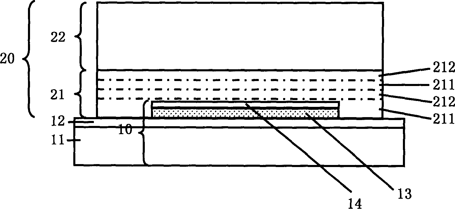
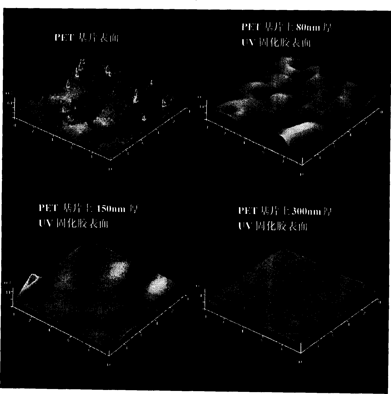
[0081] Place the OLEDs on the glass substrate in a vacuum coating machine and evacuate to 5×10 -4 pa. A layer of liquid UV-curable adhesive (UV STRCTL 352, Loctite Company) was vapor-deposited on the back of the device, and cured by ultraviolet radiation for 5 minutes. The UV-curable adhesive was in-situ polymerized into a flat solid film by ultraviolet irradiation. The film thickness was 300 nm. At a background pressure of 10 -4 ~10 -3Nitrogen gas was introduced under the condition of Pa, and the air pressure in the vacuum chamber was adjusted to 0.40Pa. The high-purity titanium target was used to sputter on the UV-curable adhesive at a DC power of 96W. The substrate temperature was controlled below 40°C, and the growth time was 10min. The thickness of the TiO thin film is 50nm. Repeat the above steps to prepare another cycle of UV curable glue / titanium nitride composite film layer. Finally, the inert gas nitrogen was introduced into the glove box, and a layer of liquid ...

Embodiment 2

[0083] Place the OLEDs on the glass substrate in a vacuum coating machine and evacuate to 4×10 -4 pa. A layer of liquid UV-curable adhesive (UV STRCTL 352, Loctite Company) was vapor-deposited on the back of the device, and cured by ultraviolet radiation for 5 minutes. The UV-curable adhesive was in-situ polymerized into a flat solid film by ultraviolet irradiation. The film thickness was 300 nm. At a background pressure of 10 -4 ~10 -3 Oxygen was introduced under the condition of Pa, and the air pressure in the vacuum chamber was adjusted to 0.40Pa. A high-purity aluminum target was used to sputter on the UV-curable adhesive at a DC power of 96W. The substrate temperature was controlled below 40°C, and the growth time was 10min. The film thickness of the aluminum thin film was 50 nm. Repeat the above steps to prepare another 2 cycles of UV curable adhesive / alumina composite film layers. Finally, the inert gas nitrogen was introduced into the glove box, and a layer of liq...

Embodiment 3

[0086] n


PUM

PropertyMeasurementUnit
thicknessaaaaaaaaaa
thicknessaaaaaaaaaa
thicknessaaaaaaaaaa

Abstract

The package layer for organic electroluminescent device is in one or two sides of the device, and includes thin film layers of alternately superposed polymer material layer and ceramic material layeras well as one thick film layer of organic insulating material on the thin film layer. The thick film layer of organic insualting material can further raise the flexibility and water and oxygen blocking performance of the package, raise mechanical performance of the device, prolong the life of the device and simplify the packing process. The method of the present invention is used for modifying plastic sheet and in preparing flexible sheet with high water and oxygen blocking performance.

Description

technical field [0001] The invention relates to an encapsulation layer of an organic electroluminescent device and a preparation method thereof, and relates to the application of the method for preparing the encapsulation layer, and belongs to the technical field of organic electroluminescence. Background technique [0002] Today, with the development of multimedia technology and the advent of the information society, the requirements for the performance of flat panel displays are getting higher and higher. In recent years, three new display technologies have emerged: plasma display, field emission display and organic electroluminescent display, all of which have made up for the shortcomings of cathode ray tubes and liquid crystal displays to a certain extent. Among them, organic electroluminescent displays have a series of advantages such as self-illumination, low-voltage DC drive, full curing, wide viewing angle, and rich colors. Low, its response speed can reach 1000 tim...

Claims


Application Information

Patent Timeline
Patent Type & Authority Applications(China)
IPC IPC(8): H01L51/52H05B33/00H05B33/04H05B33/10
CPCH01L51/5256H01L51/5237H10K50/8445
Inventor 邱勇段炼李扬王立铎
Owner TSINGHUA UNIV
Why Eureka
Try Eureka