Optoelectronic device and selection district epitaxial method of autocollimation model spot inverter integration
A mode spot converter, optoelectronic device technology, applied in laser parts, lasers, electrical components, etc., can solve the problems of loss, difficult to guarantee growth quality, etc.
- Summary
- Abstract
- Description
- Claims
- Application Information
AI Technical Summary
Problems solved by technology
Method used
Image

Examples
Embodiment 1
[0029] Example 1: Monolithic integration of a self-aligned mode spot converter and a 1.55 μm distributed feedback laser
[0030] The specific process steps are:
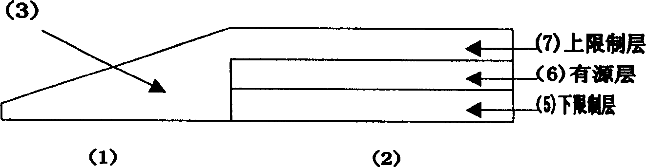
[0031] 1) On an n-type InP (indium phosphide) substrate, planarly grow an upper n-type InP buffer layer, an InGaAsP (indium gallium arsenide phosphide) lower confinement layer 5 and a compressively strained InGaAsP (indium gallium arsenide phosphide) / InGaAsP multiple quantum well layer 6( image 3 );
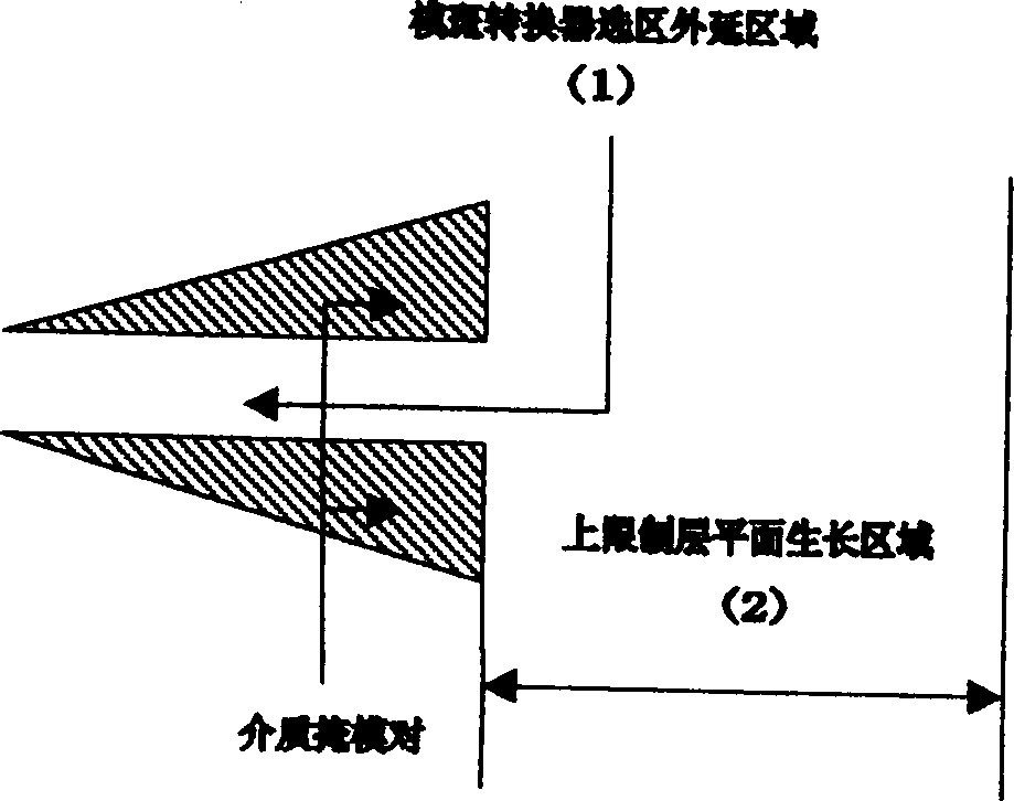
[0032] 2) Photoetch the distributed feedback laser part 2 of the device along the front mesa direction, and at the same time use selective etching technology in the spot converter area to etch the InP buffer layer with a depth of about 180nm to form a distributed feedback laser mesa ( figure 1 );
[0033] 3) 150nm SiO on planar growth 2 Dielectric mask, select epitaxial SiO by photolithography according to the optimally designed structure 2 Dielectric Mask Pattern ( figure 1 );
[0034] 4) Simultaneous planar gr...
Embodiment 2
[0045] Example 2. Monolithic integration of self-aligned waveguide mode-speckle converters and electroabsorption modulators
[0046] The modulator monolithically integrates an upper-mode speckle converter, which can reduce the insertion loss of the entire device and improve the offset tolerance of the device and fiber coupling. The specific manufacturing steps are as follows:
[0047] 1) planarly grow an upper n-type InP buffer layer, an InGaAsP lower confinement layer 5 and an InGaAsP / InGaAsP quantum well layer 6 on an n-type InP substrate, ( Figure 4 );
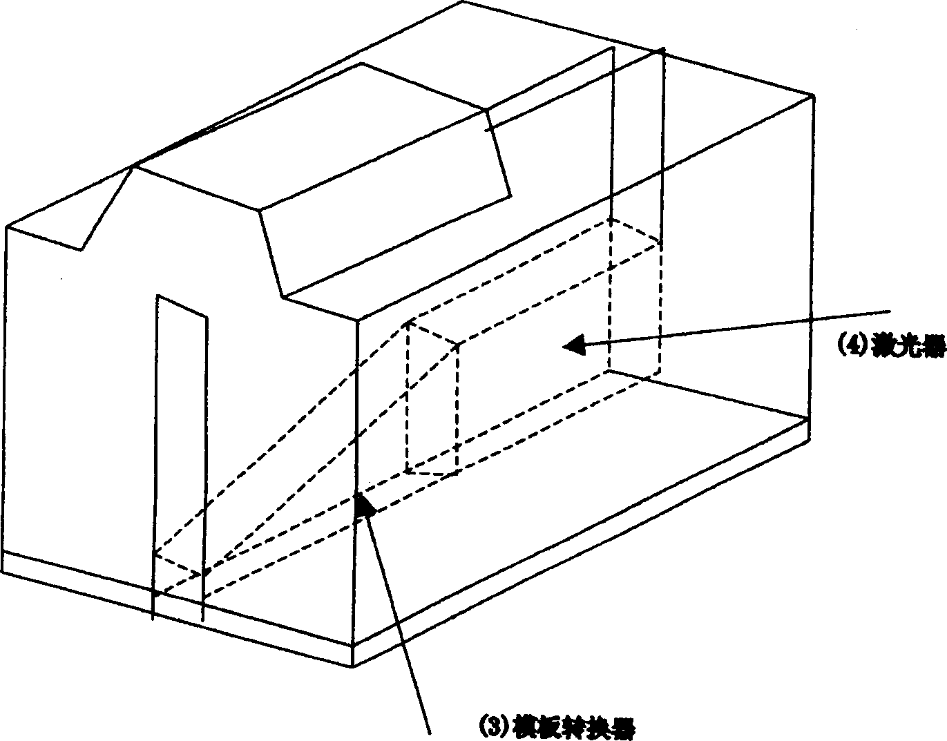
[0048] 2) The modulator part 2 is photoetched out along the front mesa direction, and the quantum well layer and the lower confinement layer of the speckle-removing converter region 1 are etched at the same time, about 280nm, and etched to the InP buffer layer to form the modulator mesa, such as figure 1 shown;
[0049] 3) 150nm SiO on planar growth 2 Dielectric mask, select the epitaxial pattern according to the optima...
PUM
 Abstract
Description
Claims
Application Information
 - R&D
- Intellectual Property
- Life Sciences
- Materials
- Tech Scout
- Unparalleled Data Quality
- Higher Quality Content
- 60% Fewer Hallucinations
Browse by: Latest US Patents, China's latest patents, Technical Efficacy Thesaurus, Application Domain, Technology Topic, Popular Technical Reports.
© 2025 PatSnap. All rights reserved.Legal|Privacy policy|Modern Slavery Act Transparency Statement|Sitemap|About US| Contact US: help@patsnap.com