Spot diffraction interferometer for measuring surface shape

A technology of point diffraction interferometer and surface shape, which is applied in the fields of interference spectroscopy, phase influence characteristic measurement, spectrum investigation, etc. It can solve the problems of affecting the accuracy of measurement results, increasing the difficulty of instrument assembly, and low light transmittance of small holes. , to achieve good focusing effect, easy assembly and adjustment, and large numerical aperture

Inactive Publication Date: 2003-07-23
SHANGHAI INST OF OPTICS & FINE MECHANICS CHINESE ACAD OF SCI
View PDF0 Cites 17 Cited by
  • Summary
  • Abstract
  • Description
  • Claims
  • Application Information

AI Technical Summary

Problems solved by technology

In the prior art, etching and other methods are used to make small holes. This method is difficult to make ideal small holes, so the diffracted light waves are no longer ideal spherical waves.
This will seriously affect the accuracy of the measurement results, and the irradiation spot is not small enough, and the light transmittance of the small hole is low, which also affects the detection accuracy
At the same time, it is very difficult to make the light spot incident on the small hole with wavelength order, which increases the difficulty of instrument assembly, poor repeatability and high detection cost

Method used


Image

  • Spot diffraction interferometer for measuring surface shape
  • Spot diffraction interferometer for measuring surface shape
  • Spot diffraction interferometer for measuring surface shape

Examples


Embodiment 1

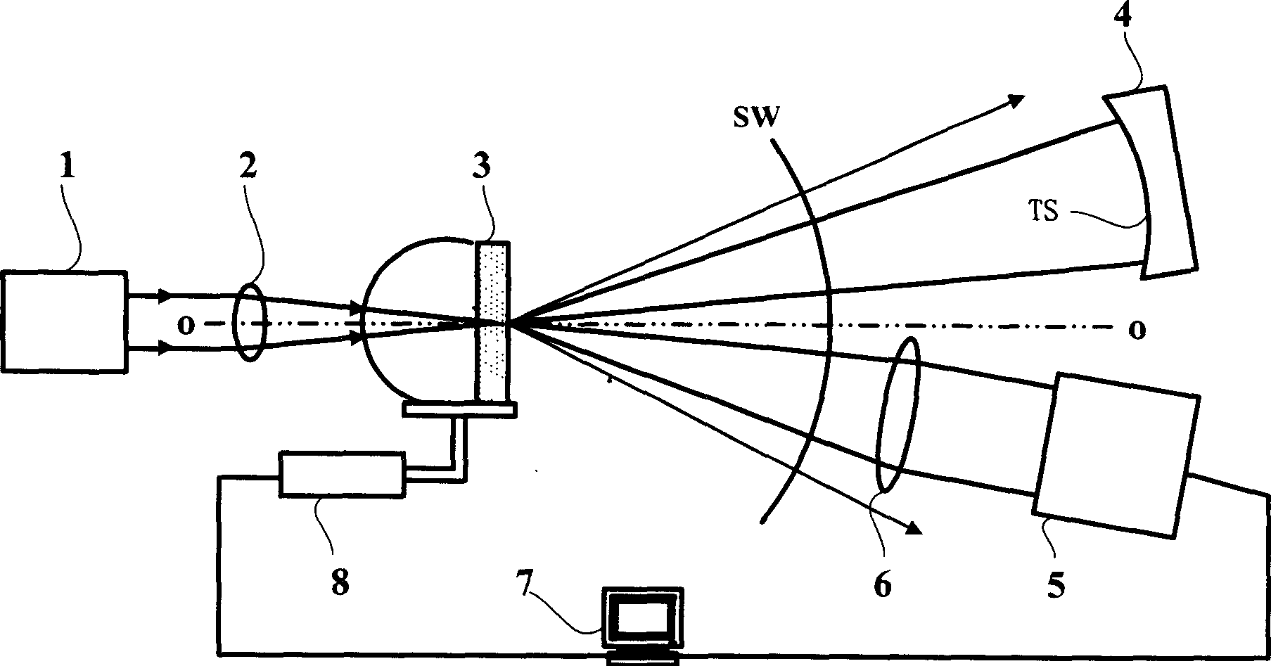
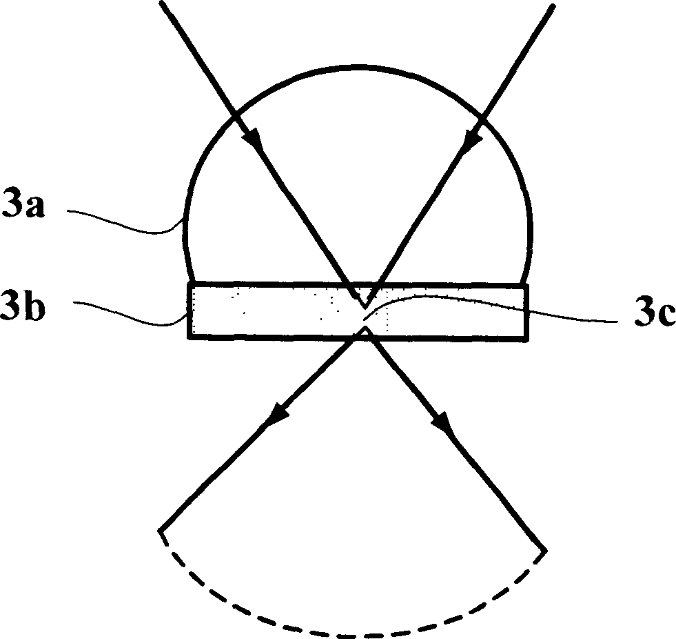
[0035] The schematic diagram of its device structure is shown in figure 1As shown, the light source 1 is a semiconductor laser with a wavelength λ=650nm. The converging lens 2 has a numerical aperture of 0.9 and a working distance of 3 mm. The solid immersion lens 3 a has a radius of 0.764 mm, is made of glass with a refractive index of 1.8198 at 514.5 nm, and has a numerical aperture of 1.5. By adjusting the displacement control device 8, the focus spot falls on the super-resolution mask 3b. The device under test is placed on the piezoelectric ceramic base, and the distance between the device under test 4 and the solid wetting lens 3 is adjusted until clear stripes are obtained on the CCD camera 5 . Collect the data to the computer 7 to complete a measurement.

Embodiment 2

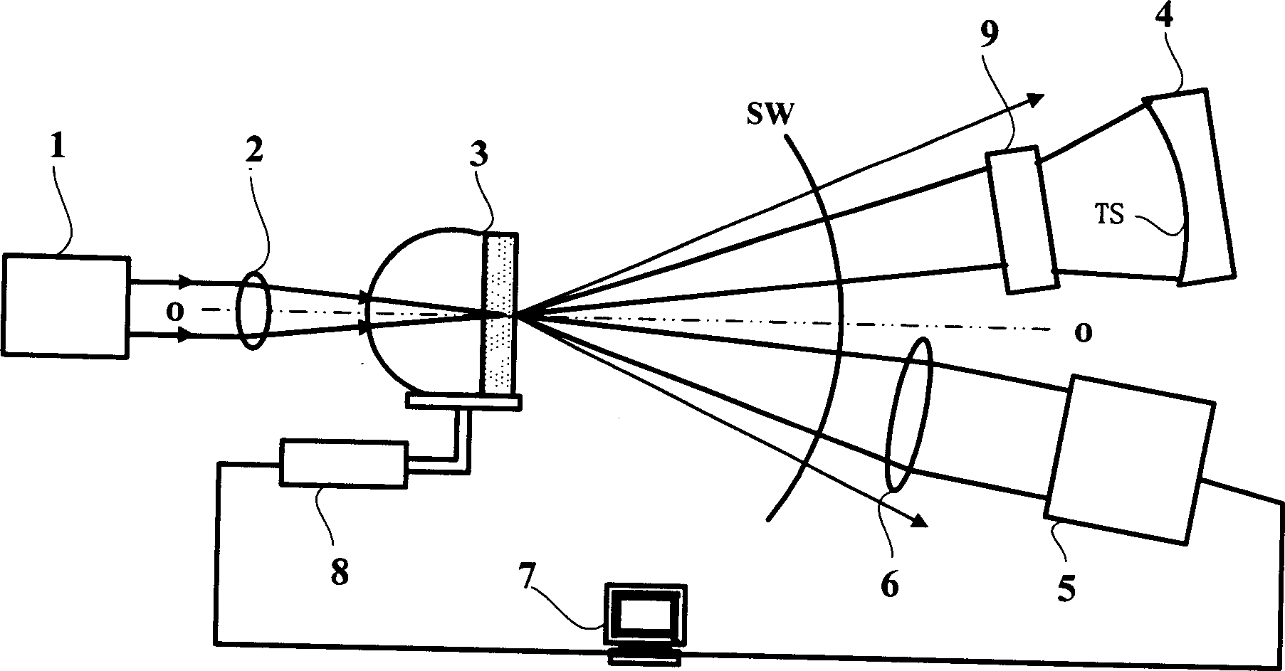
[0037] The schematic diagram of its device structure is shown in image 3 As shown, the devices with the same numbers as those in Embodiment 1 will not be described in detail here. The compensator (NULL element) 9 is placed between the small hole 3c and the device under test 4 to generate a wavefront close to the TS on the entire surface TS of the device under test 4, to solve the problem that the surface TS of the device under test 4 is very different from the ideal spherical surface When the case is large, that is, the case of an aspheric surface, the entire measurement can be completed once. Its accuracy depends on the quality of the compensator 9 .

[0038] The compensator 9 may be a spherical transmissive optical device, a spherical reflective optical device, an aspheric transmissive optical device or an aspheric reflective optical device.

Embodiment 3

[0040] Its device structure is as Figure 4 As shown, the devices with the same numbers as those in Embodiment 1 will not be described in detail here. Light emitted from the light source 1 is split by a beam splitter 12 into a measurement beam and a reference beam. The reference beam passes through a beam splitter 12 to a movable mirror 10 . The optical path difference between the reference beam and the measurement beam can be adjusted by moving the mirror 10 . The reference beam passes through the beam splitter 12 again, is reflected by the mirror 13 to the converging lens 2 , and then is focused to the solid immersion lens 3 by the converging lens 2 . At the same time, the measuring beam is reflected by the beam splitter 12 and encounters the fixed mirror 11 . The measuring beam is reflected back to the beam splitter 12 . Then reflected to the mirror 13, the mirror 13 reflects the measuring beam to the converging lens 2, and is focused by the converging lens 2 to the sol...


PUM

PropertyMeasurementUnit
radiusaaaaaaaaaa
refractive indexaaaaaaaaaa

Abstract

The interferometer includes the optical part and the data acquisition, process and control parts. The optical part includes the laser, the convergent lens, the lens soaked by the solid coated with super resolving power mask arranged in optical axis in sequence along the traveling direction of the laser beam. The part to be measured is positioned above the optical axis and the image lens is in lower part. The data acquisition, process and control parts include the CCD camera, the computer and the displacement controller. The key technique in the invention is the lens soaked by the soild and the mask with supper resolving power. Thus, the smaller pinhole can be obtained as the ideal light source with spherical wave. The position and size of the pinhole are adjustable, providing high transmittance of light and low requirement for the quality of the light beam.

Description

Technical field: [0001] The invention relates to optical surface detection and is a device for detecting the surface shape of a device with high precision. In particular, a point-diffraction interferometer employing a solid immersion lens and a super-resolution mask. Background technique: [0002] The traditional method of inspecting the quality of optical surfaces such as spheres is to use Fizeau interferometer or Tyman-Green interferometer. These methods require an actual reference surface, which means that the traditional method of evaluating the quality of the surface shape of a device under test is to compare it with an actual reference surface that is regarded as ideal. For large optical devices, such as the mirrors of astronomical telescopes, which can be more than 1 meter in diameter, it is almost impossible to manufacture such a large reference surface. Moreover, the measurement accuracy of traditional methods cannot exceed the accuracy of the reference surface. F...

Claims


Application Information

Patent Timeline
Patent Type & Authority Applications(China)
IPC IPC(8): G01J3/45G01N21/45
Inventor 徐文东周飞王阳张锋魏劲松
Owner SHANGHAI INST OF OPTICS & FINE MECHANICS CHINESE ACAD OF SCI
Why Eureka
Try Eureka