Anode welding process for metal-glass and metal-ceram
A glass and metal technology, applied in the field of connection of heterogeneous materials, can solve problems such as the limitation of welding range
- Summary
- Abstract
- Description
- Claims
- Application Information
AI Technical Summary
Problems solved by technology
Method used
Image
Examples
Embodiment 1
[0034] Example 1: Aluminum-K 4 Anodic welding of glass
[0035] Material Composition:
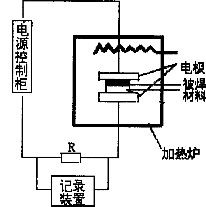
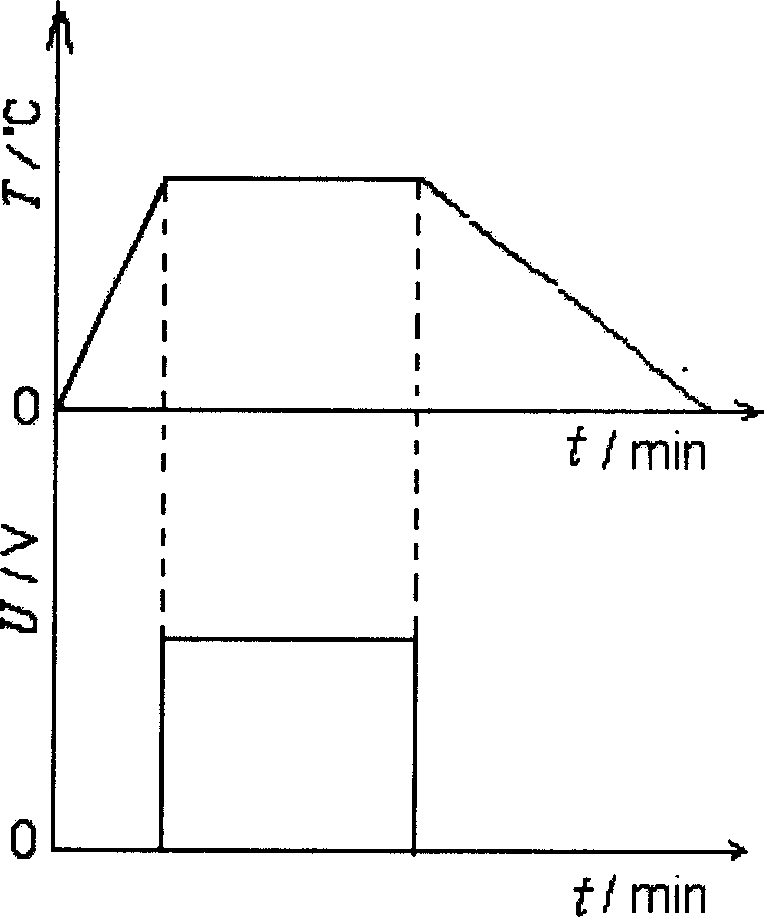
[0036] The experimental material is K 4 Glass and pure aluminum, the size of glass and aluminum sheet is 12mm×12mm, the surface needs to be mechanically polished, and cleaned in acetone and alcohol respectively. welding process in figure 1 The welding in the atmosphere is carried out in the experimental equipment shown, and it is cooled to room temperature with the furnace after welding.
[0037] Within the optimal process parameters (temperature 250°C-400°C, voltage 600V-800V), the welding rate is over 90%. The test shows that the welding rate increases with the increase of temperature and voltage. The effect of the elevated temperature is to detach the weaker-connected ions in the glass and move directionally under the action of the electric field. An increase in temperature is conducive to ion diffusion. However, as the temperature increases, the thermal expansion coefficient misma...
Embodiment 2
[0040] Example 2: Kovar-K 4 Anodic welding of glass
[0041] Kovar alloy has a linear expansion coefficient similar to that of borosilicate glass at 20°C to 450°C and good low-temperature stability. During the welding process with metals, it can reduce the thermal stress caused by the different thermal expansion coefficients of dissimilar materials. . The welding parts of this alloy and glass are mainly used in electric vacuum components, such as launch tubes, oscillators, sealing plugs, magnetrons, etc.
[0042] K 4 The glass sample size is 10mm×10mm×2mm, and the Kovar alloy sample size is 10mm×10mm×15mm.
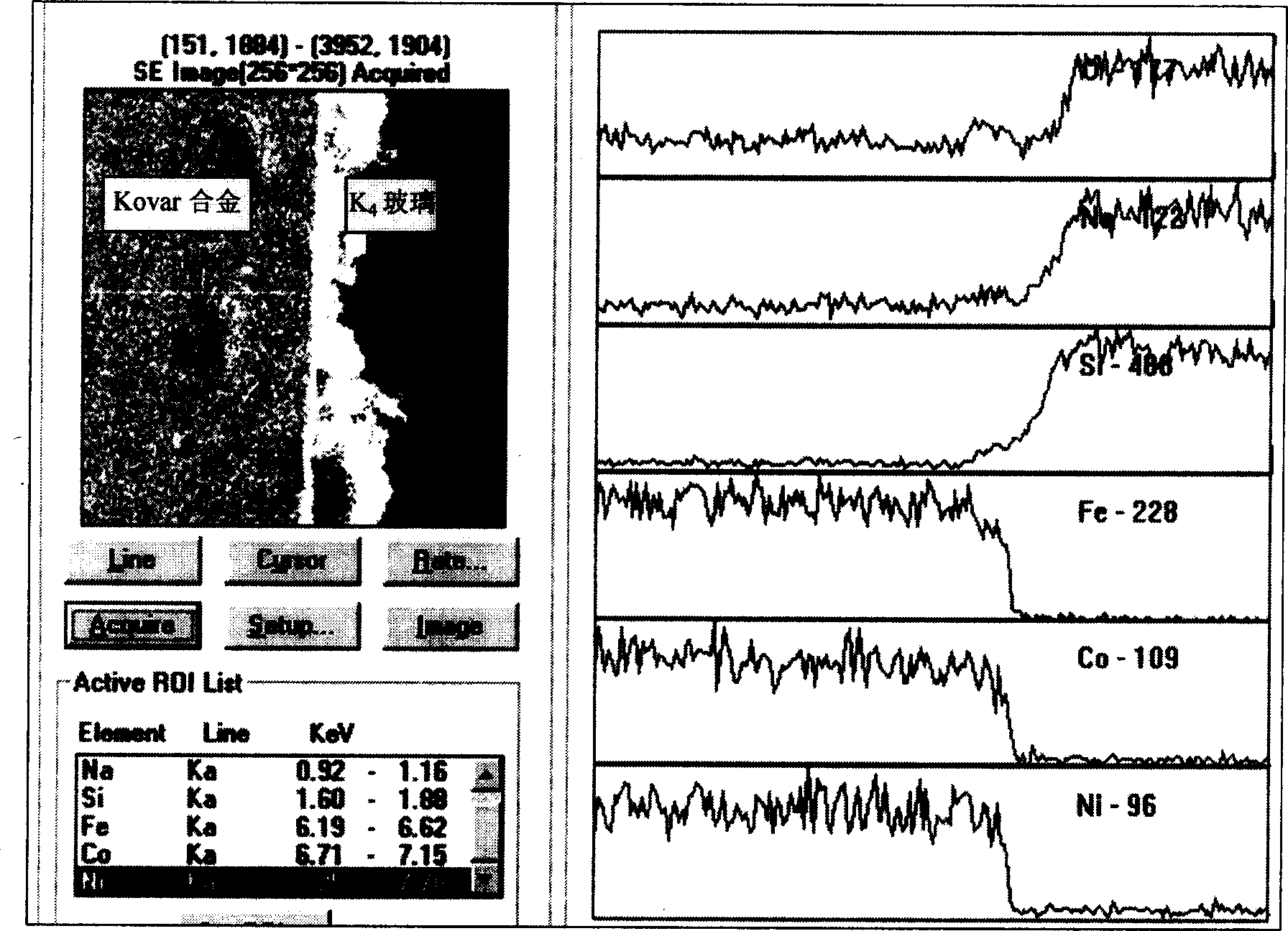
[0043] The test process will K 4 The surface of glass and Kovar alloy is polished on one side, and the surface roughness reaches 0.5 μm to 1.0 μm, and then cleaned with acetone and alcohol, and the two polished surfaces are relatively attached, and assembled in a fixture, wherein the Kovar alloy is connected to the anode , K 4 The glass is connected to the cathode, s...
Embodiment 3
[0047] Embodiment 3: anodic welding of K4 glass and monocrystalline silicon chip
[0048] K 4 The sample size of the glass is 10mm×10mm×2mm. The sample size of the single crystal Si wafer is 10mm×10mm×0.3mm.
[0049] The welding test device and process samples are surface polished (roughness 0.5-1.0 μm) and surface cleaned (clean the surface with acetone and alcohol) before assembly. After the two samples are assembled, they are put into the furnace, and the silicon wafer and the anode connected, and the glass is connected to the cathode. After the sample is heated to a temperature of 350°C to 400°C, apply a DC voltage of 710V to 840V to the sample to be welded, keep it for 15 to 50 minutes, disconnect the power supply, and cool the sample with the furnace.
[0050] During the welding process, the test system is used to record the change of the current, and it is found that the welding current rises monotonously to a maximum value and then decreases slowly. During the weld...
PUM
| Property | Measurement | Unit |
|---|---|---|
| surface roughness | aaaaa | aaaaa |
| tensile strength | aaaaa | aaaaa |
Abstract
Description
Claims
Application Information


