Method for making semiconductor laser and spot-size converter by double waveguide technology

A mode spot converter and laser technology, which is applied in the direction of semiconductor lasers, lasers, laser components, etc., can solve the problems of small process tolerance, deterioration of mode characteristics, and low reliability of devices, so as to reduce Auger recombination and reduce Noise index, the effect of reducing the number of growth

Inactive Publication Date: 2006-04-05
INST OF SEMICONDUCTORS - CHINESE ACAD OF SCI
View PDF0 Cites 13 Cited by
  • Summary
  • Abstract
  • Description
  • Claims
  • Application Information

AI Technical Summary

Problems solved by technology

The three mode spot converters have their own advantages and disadvantages: the thickness of the vertical wedge-shaped waveguide changes gradually from the active area to the output end face
[0005] Although there are many reports on monolithic integrated devices of lasers and spot converters in the world, the following disadvantages generally exist: 1) The laser adopts a buried structure, the number of epitaxy increases, the process is complicated, and the reliability of the device is low
2) The mold spot converter adopts vertical wedge shape, adopts butt-joint (that is, docking) epitaxy technology or gradual cor...

Method used


Image

  • Method for making semiconductor laser and spot-size converter by double waveguide technology
  • Method for making semiconductor laser and spot-size converter by double waveguide technology
  • Method for making semiconductor laser and spot-size converter by double waveguide technology

Examples


Embodiment

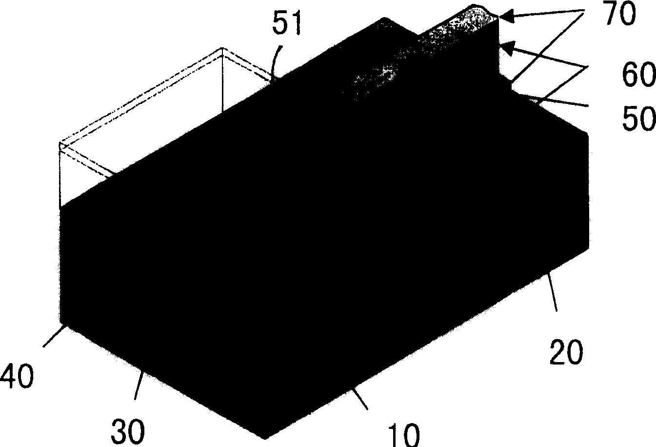
[0065] The invention relates to a novel method for making LD-SSC. It is characterized in that it comprises the following manufacturing steps:

[0066] (1) The 2-inch n-InP substrate undergoes strict decontamination (heating and boiling with ethanol, trichlorethylene, acetone, and ethanol in sequence) → pickling (soaking in concentrated sulfuric acid for 1 to 2 minutes) → water washing (rinsing with deionized water More than 50 times) → after drying treatment, put it into the growth chamber, the growth temperature is 655°C, the growth pressure is 22mbar, and the graphite boat speed is 75~80 rpm. The growth rate is 0.4~0.7nm / s.

[0067] (2) On the n-type indium phosphide substrate (100) epitaxially grow n-type indium phosphide buffer layer (0.5 μm thick), lower waveguide layer (thickness 50nm, bandgap wavelength 1.1 or 1.2 μm), 0.2 μm Indium phosphide space layer, lower optical confinement layer (thickness 80nm, bandgap wavelength 1.1 or 1.2μm), compressive strain active regio...


PUM

PropertyMeasurementUnit
Thicknessaaaaaaaaaa
Bandgap wavelengthaaaaaaaaaa
Thicknessaaaaaaaaaa

Abstract

Disclosed a method for utilizing the dual-waveguide technology to manufacture the semiconductor laser and mode spot switch comprises following steps: on the N type indium phosphide substrate, sequentially extending growing the N type indium phosphide breaker, a lower waveguide layer, a space layer, a active region, and a thinner indium phosphide intrinsic layer, wherein, the indium phosphide intrinsic layer can prevent the oxidation of active region; removing the highest indium phosphide intrinsic layer, partly covering the laser with SiO2, and utilizing the wet corrosion process to etch the upper carinate shape of mode spot switch; utilizing the auto-alignment process to etch the lower carinate shape which comprises a lower waveguide layer, a space layer, a second growth P type indium phosphide coating layer, and a high doping P type indium gallium arsenide ohmic electrode contract layer; utilizing the SiO2 to partly cover the mode spot switch and etching the upper and lower carnate shapes again while the upper carinate shape comprises a active region, a P type indium phosphide coating layer and a high doping P type indium gallium arsenide ohmic electrode contract layer; and decreasing the substrate of extended plate to 100 ª–m, and manufacturing P/N electrodes to be scribed into the tube core of 250í‡500ª–m.

Description

technical field [0001] The invention relates to a method for manufacturing a semiconductor laser and a mode-spot converter by using a novel double-waveguide technology by conventional wet etching and photolithography techniques. Background technique [0002] Most modules in optical fiber communication systems are composed of III-V compound semiconductor devices. Each semiconductor device must be connected to at least one optical fiber, so the coupling efficiency between the semiconductor optoelectronic device and the optical fiber is very important. For ordinary glass optical fibers, the refractive index difference between the core layer and the cover layer is very small, generally 5×10 -3 the following. Such a waveguide structure is a weakly guided waveguide, and the distribution of its intrinsic light field is quite diffuse, that is, the intrinsic light spot is relatively large, generally with a diameter of about 8-10 μm. In III-V compound semiconductors, if the refract...

Claims


Application Information

Patent Timeline
IPC IPC(8): H01S5/00
Inventor 侯廉平王圩
Owner INST OF SEMICONDUCTORS - CHINESE ACAD OF SCI
Why Eureka
Try Eureka