Preparation method of GaN based laser diode with naturally cleaved cavity surface

A laser diode and natural cleavage technology, which is applied in the field of GaN-based laser diode chip preparation, can solve the problems of poor electrical conductivity and difficulty in preparing natural cleavage planes, and achieve the effect of ensuring uniformity

Inactive Publication Date: 2006-07-26
DONGGUAN INST OF OPTO ELECTRONICS PEKING UNIV
View PDF0 Cites 5 Cited by
  • Summary
  • Abstract
  • Description
  • Claims
  • Application Information

AI Technical Summary

Problems solved by technology

The feature of the invention is that it simultaneously solves the difficulties of poor thermal conductivity and electrical conductivity and difficulty in preparing natural cleavage planes in current gallium nitride-based lasers

Method used


Image

  • Preparation method of GaN based laser diode with naturally cleaved cavity surface
  • Preparation method of GaN based laser diode with naturally cleaved cavity surface
  • Preparation method of GaN based laser diode with naturally cleaved cavity surface

Examples


Embodiment 1

[0026] The technical scheme of embodiment one:

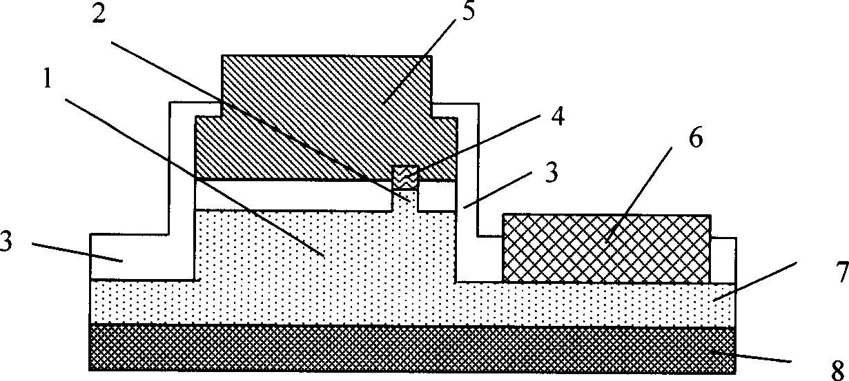
[0027] (a) On the GaN-based LD epitaxial wafer of the sapphire substrate, first etch a P-type mesa 1 with a height of 1.5 μm-2.5 μm; then etch a ridge-shaped waveguide region 2 on the P-type mesa 1 with a height of 0.2 μm-0.8 μm, deposit an oxide insulating layer 3 on the P-type mesa, and deposit a Ni / Au (20nm / 20nm) P-type ohmic contact layer 4 in it after corroding the P-type electrode window. Deposition of Au (30nm / 400nm) 5, then etch the electrode window on N-type GaN 7 and deposit N-type electrode Ti / Al / Ti / Au (30nm / 150nm / 30nm / 400nm) layer 6, 400°C under nitrogen atmosphere After one minute the alloy forms the basic structure of the laser diode, as Figure 1a and 1b ;

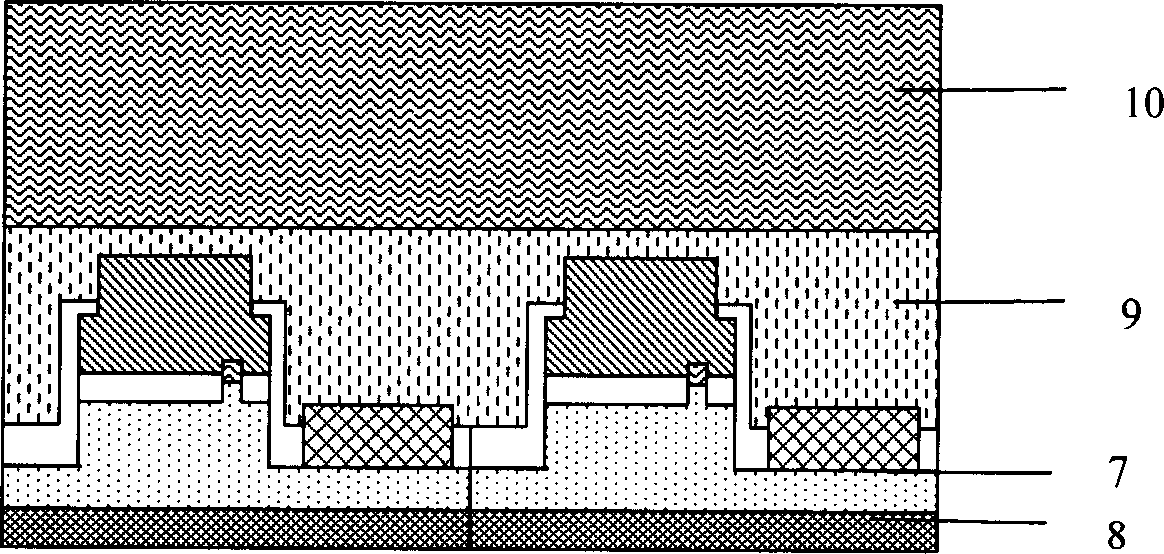
[0028] (b) Apply organic glue 9 on one side of the P-type metal thickened electrode and adhere to the cleaned Si substrate 10, then put it into a vacuum chamber to evacuate, remove air bubbles to ensure the uniformity and smoothness of bonding, as shown in F...

Embodiment approach 2

[0036] Embodiment two of the present invention are as follows (concrete steps are as Fig. 3):

[0037] (a) On the GaN-based LD epitaxial wafer of the sapphire substrate, first etch a P-type mesa 1 with a height of 1.5 μm-2.5 μm; then etch a ridge-shaped waveguide region 2 on the P-type mesa 1 with a height of 0.2 μm-0.8 μm, deposit an oxide insulating layer 3 on the P-type mesa, and deposit a Ni / Au (20nm / 20nm) P-type ohmic contact layer 4 in it after corroding the P-type electrode window. Deposition of Au (30nm / 400nm) 5, followed by alloying at 400°C for one minute under nitrogen atmosphere, as Figure 3a ;

[0038] (b) Apply organic glue 9 on one side of the P-type metal thickened electrode and adhere to the cleaned Si substrate 10, then put it into a vacuum chamber to evacuate to ensure the uniformity and firmness of the bonding, such as Figure 3b

[0039] (c) After the LD epitaxial wafer bonded to the Si wafer is irradiated by the KrF excimer laser 11, the sapphire subs...


PUM

PropertyMeasurementUnit
Thicknessaaaaaaaaaa

Abstract

This invention provides one method to process GaN extending layer natural deavage surface as laser chamber lens by use of metal Cu as chop hot deposition and supportive underlay to improve laser chamber lens optical quality and the parts integrated property index to omit polishing and dividing procedures. This invention has GaN and LD laser tube core structure not eh GaN extending slice with same isolation and circle to the laser tube core and uses deavage laser as supporting and as LD chip final deposition.

Description

technical field [0001] The invention belongs to the field of photoelectric technology, and specifically relates to the preparation technology of a GaN-based laser diode (LD) chip. It includes the use of a laser with a wavelength shorter than the GaN bandgap absorption wavelength to peel off the GaN-based LD epitaxial layer grown on a sapphire substrate, and on this basis to prepare an LD chip with a GaN natural cleavage plane as the laser cavity mirror. Background technique [0002] Most of the current GaN-based laser diode (LD) devices are epitaxially grown on sapphire substrates (mismatch up to 15%) with a large lattice mismatch with GaN materials, which leads to a high dislocation density in the active region of 1 ×10 8 / cm 2 At the same time, due to the inherent properties of GaN-based materials, a series of technical difficulties have been brought about for material growth and device fabrication. These mainly include difficult cleavage of the cavity mirror, difficult...

Claims


Application Information

Patent Timeline
IPC IPC(8): H01S5/323
Inventor 康香宁胡晓东王琦章蓓杨志坚徐科陈志忠于彤军秦志新张国义
Owner DONGGUAN INST OF OPTO ELECTRONICS PEKING UNIV
Why Eureka
Try Eureka