

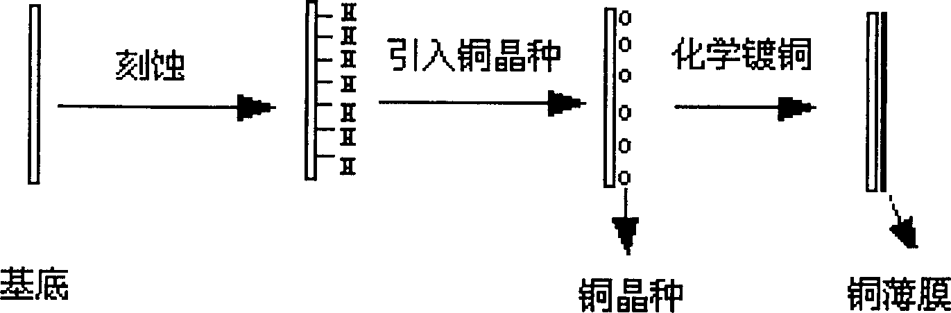
Process for electroless copper on silicon chip
A technology of electroless copper plating and silicon wafer, which is applied in the direction of liquid chemical plating, metal material coating process, coating, etc., can solve the problem of high cost, and achieve the goal of avoiding impurity metal, improving purity and conductivity, and low price Effect
- Summary
- Abstract
- Description
- Claims
- Application Information
AI Technical Summary
Problems solved by technology
Method used
Image

Examples
Embodiment 1
[0015] Embodiment 1: electroless copper plating on silicon chip
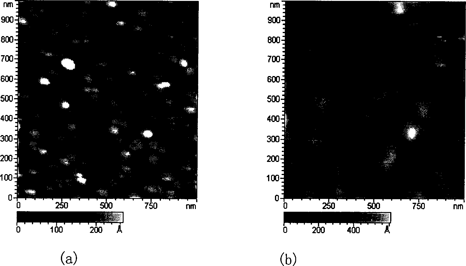
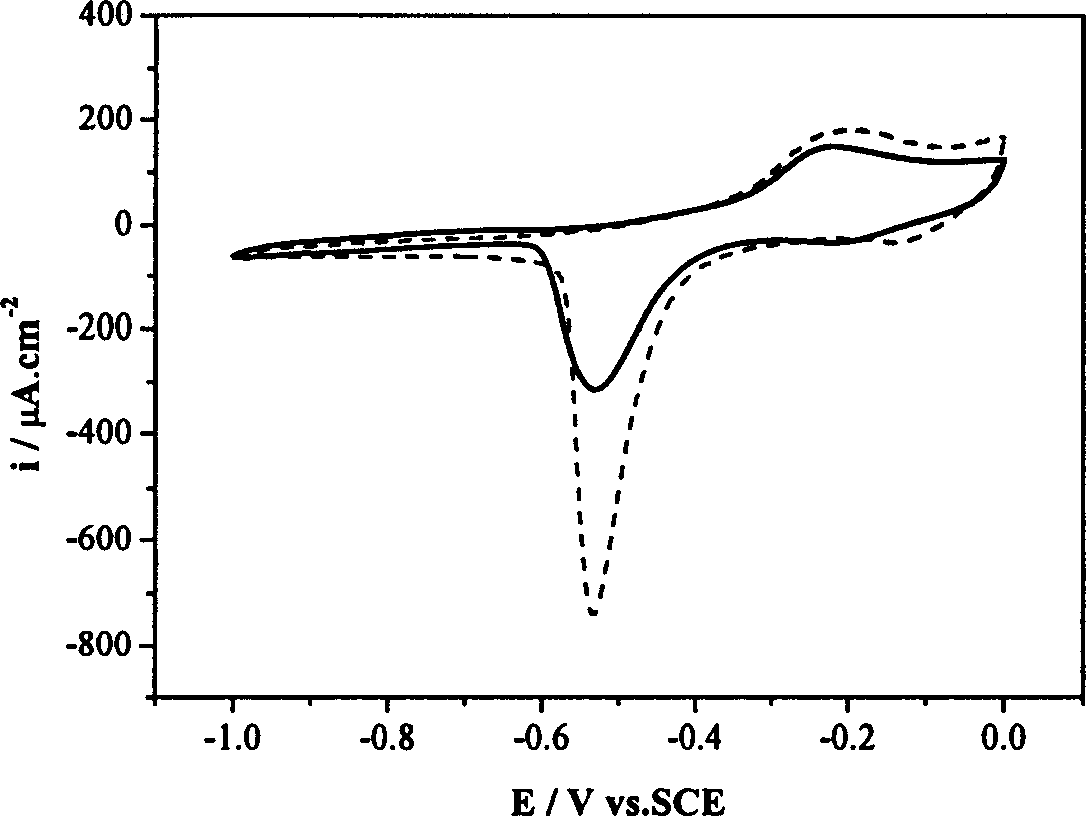
[0016] The monocrystalline silicon wafer (5-10Ωcm -1 ) plane polishing, followed by alternating ultrasonic cleaning with acetone and water three times each. Clean the surface of the silicon wafer with a mixture of sulfuric acid and hydrogen peroxide. Etch the silicon wafer in ammonium fluoride and hydrofluoric acid buffer solution for 1-5min, and rinse the surface with ultrapure water. Place the polished, cleaned and etched silicon wafer in a hydrofluoric acid solution containing copper sulfate, take it out after 5s-5min, and rinse it with ultrapure water. Then placed in the electroless copper plating solution, the solution components are 1-25g / L copper sulfate, 5-125g / L potassium sodium tartrate, 2-50mL / L formaldehyde, 1.4-35g / L sodium hydroxide; the solution pH is 12.5 ~13, room temperature, copper plating time is 10-30 minutes.
PUM
 Abstract
Description
Claims
Application Information