Process for preparing nano ZnO

A nanostructure and nanocomb technology, which is applied in nanostructure manufacturing, nanotechnology, nanotechnology, etc., can solve problems such as poor controllability, high temperature requirements, and process incompatibility, and achieve simple methods, low cost, and mild conditions. Effect

Inactive Publication Date: 2006-12-27
EAST CHINA NORMAL UNIV
View PDF0 Cites 18 Cited by
  • Summary
  • Abstract
  • Description
  • Claims
  • Application Information

AI Technical Summary

Problems solved by technology

The cost of molecular beam epitaxy is too high to meet the requirements of large-scale production; chemical vapor deposition is a relatively good method, but the controllability of nanostructures needs to be improved; although the solution synthesis method can be used at a lower temperature ZnO nanostructures are grown, but they are incompatible with traditional semiconductor processes; thermal evaporation has become one of the main methods for preparing ZnO nanostructures due to its low cost, easy operation, and ability to prepare various morphologies, but its disadvantages Because of: high temperature requirements, poor controllability
Another method for preparing ZnO nanostructures, top-down, has not been reported so far

Method used


Image

  • Process for preparing nano ZnO
  • Process for preparing nano ZnO
  • Process for preparing nano ZnO

Examples


Embodiment 1

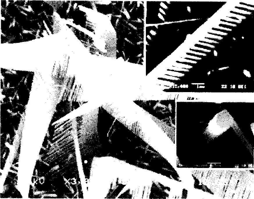
[0022] A. Synthesis of ZnO nanocomb structure and ZnO nanorods

[0023] 1) First, the silicon wafer is polished with fine sandpaper to make the surface rough and provide nucleation points for growth materials.

[0024] 2) sequentially use 1:3 concentrated sulfuric acid and hydrogen peroxide (concentration is 30%), 1:3:3 ammonia water (concentration is 27%), hydrogen peroxide and deionized water; and 1:3:3 hydrochloric acid (concentration is 38%), hydrogen peroxide and deionized water (both in volume ratio) were heated and cleaned with a heating furnace to clean the polished silicon wafer for about 8 minutes each.

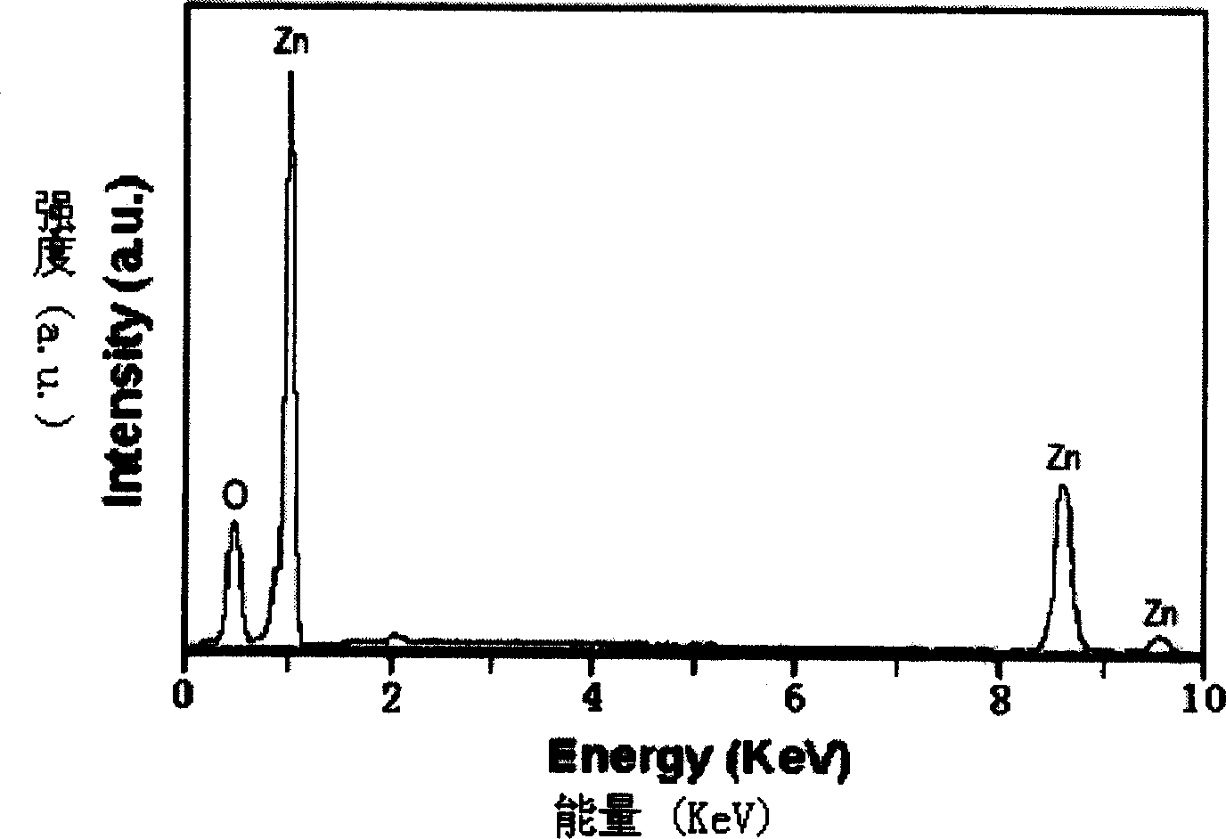
[0025] 3) Zn (purity 99.99%) powder is placed on a quartz boat, and then a layer of mixture of zinc oxide and graphite powder is covered on it. Place the cleaned silicon wafer on the mixture of the three, and the vertical distance between them is about 1mm.

[0026] 4) Heat the furnace to 650°C and keep it for a few minutes, then place the prepared quartz boat in ...

Embodiment 2

[0035] A. Synthesis of ZnO nanocomb structure and ZnO nanorods

[0036] Same as step A of embodiment 1

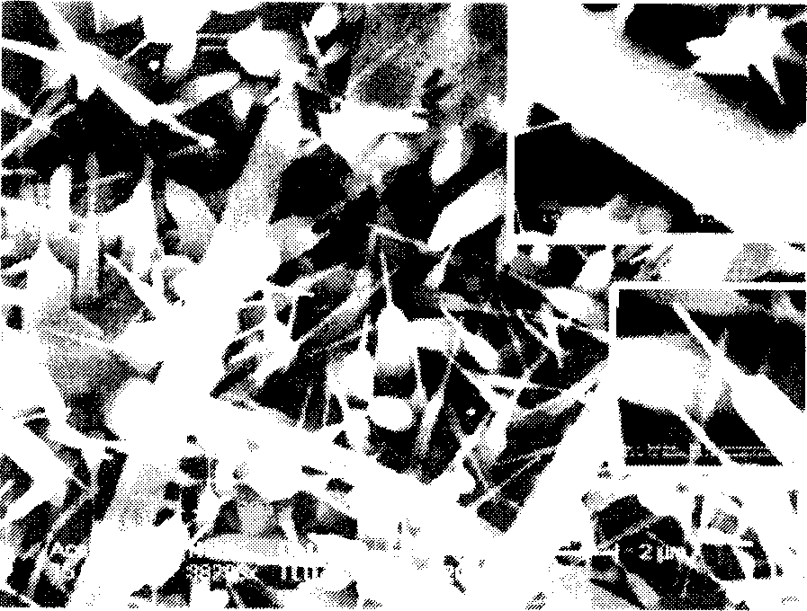
[0037] B. Dissolve 1.0 g of thiourea in 100 ml of deionized water as a spare solution. Then put the silicon chip with ZnO nanostructure synthesized by thermal evaporation into the standby solution. After keeping at room temperature for 15 hours, take out the silicon wafer and wash it several times with deionized water, and finally dry it in an oven at 95°C. The etching principle is that thiourea dissolves in deionized water and undergoes a reversible reaction to produce weak hydrogen sulfuric acid. the essence lies in , thus realizing the etching of ZnO nanostructures.

Embodiment 3

[0039] A. Synthesis of ZnO nanocomb structure and ZnO nanorods

[0040] Same as step A of embodiment 1

[0041] B. Dissolve 1.3g of thiourea in 100ml of deionized water as a spare solution. Then put the silicon chip with ZnO nanostructure synthesized by thermal evaporation into the standby solution. After keeping at room temperature for 8 hours, take out the silicon wafer and wash it several times with deionized water, and finally dry it in an oven at 95°C. The etching principle is that thiourea dissolves in deionized water and undergoes a reversible reaction to produce weak hydrogen sulfuric acid. the essence lies in , thus realizing the etching of ZnO nanostructures.


PUM

PropertyMeasurementUnit
diameteraaaaaaaaaa
lengthaaaaaaaaaa

Abstract

The invention discloses a preparing method of ZnO nanometer structure etched by sulfourea solution; which comprises the following steps: synthesizing ZnO nanometer comb-shaped structure and nanometer bar through traditional heat-growth method; etching through sulfourea solution; preparing ZnO nanometer needle-tube structure and nanometer band shaped structure; dissolving sulfourea in the deionized water to proceed reversible reaction to produce weak hydrosulfuric acid. The reaction formula is that ZnO+H+-Zn++H2O to realize bottom-up and top-down ZnO nanometer structure. The invention is convenient to control diameter of nanometer line and thickness with low cost, which is compatible with micro-electronic technology.

Description

technical field [0001] This patent belongs to the field of semiconductor nanomaterial preparation, and specifically relates to a method for preparing ZnO nanostructures by etching with thiourea solution, and in particular to propose a method opposite to the traditional bottom-up method, that is, top-up A top-down method to prepare ZnO nanostructures. technical background [0002] The preparation methods of nanomaterials are mainly divided into two ways: top-down (top-down) and bottom-up (bottom-up). The top-down approach is to use bulk crystals to obtain nanomaterials through corrosion, etching or grinding. Bottom-up is to start from atoms or molecules to control, assemble or chemically react to generate nanomaterials or nanostructures. As a wide bandgap semiconductor compound, ZnO has unique optical, electrical, photoelectric and piezoelectric properties, and has been widely used in optoelectronic devices, solar cell optical waveguides, power devices and sensors. So far,...

Claims


Application Information

Patent Timeline
Patent Type & Authority Applications(China)
IPC IPC(8): C01G9/02B82B3/00
Inventor 白伟张秋香郁可朱自强
Owner EAST CHINA NORMAL UNIV
Why Eureka
Try Eureka