Indium oxide/cerium oxide sputtering target, transparent conductive film and process for producing transparent conductive film

一种透明导电膜、氧化铈的技术,应用在溅射靶领域,能够解决难以使用、细化、Al配线断线等问题

Inactive Publication Date: 2007-03-14
IDEMITSU KOSAN CO LTD
View PDF9 Cites 13 Cited by
  • Summary
  • Abstract
  • Description
  • Claims
  • Application Information

AI Technical Summary

Problems solved by technology

[0013] (4) Full color is also easy
As a result, the Al wiring may be disconnected or "line thinning" may occur
On the other hand, IZO (Indium-Zinc Oxide: "IZO" is a registered trademark) can be considered as an amorphous material. In the case of a structure with a reflective electrode on a transparent electrode, it is difficult to use

Method used


Image

  • Indium oxide/cerium oxide sputtering target, transparent conductive film and process for producing transparent conductive film

Examples


Embodiment 1

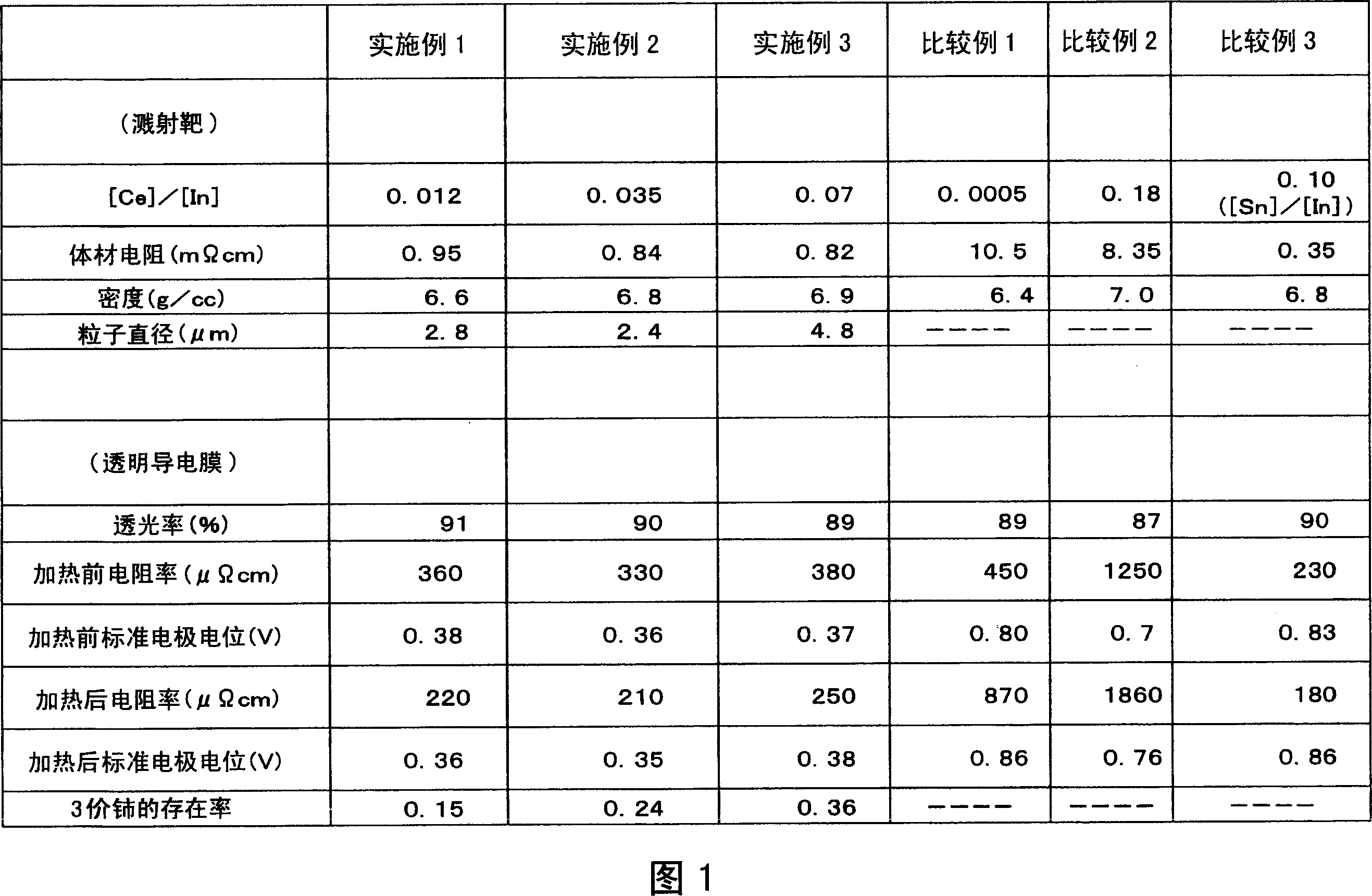
[0091] In the average particle size below 1μm 2 o 3 Powder and CeO with an average particle size below 1 μm 2 The powder was blended so that the atomic number ratio of cerium / indium reached 0.012, and it was added to a resin pot, and pure water was added to conduct a test using hard ZrO 2 Ball mill for wet ball mill mixing. The mixing time was set to 20 hours.

[0092] As a result of the mixing, the obtained mixed slurry was taken out, filtered, dried and granulated. Apply 294MPa (3t / cm 2 ) pressure, using a low-temperature static pressure press to form.

[0093] Then, the molded body was sintered as shown below.

[0094] First, in the sintering furnace, form a furnace volume per 0.1m 3An atmosphere of oxygen was introduced at a rate of 5 L / min. Sintering was carried out at 1450° C. for 8 hours in this atmosphere. At this time, the temperature was raised to 1000°C at 1°C / min, and at 2°C / min for 1000 to 1450°C. Thereafter, oxygen introduction was stopped, and the temp...

Embodiment 2

[0106] In this Example 2, except that the ratio of the number of atoms of cerium and indium per unit volume and unit mass ((number of cerium atoms) / (number of indium atoms)) was adjusted to 0.035, the same method was carried out. The same processing and operation as described in Example 1.

[0107] As a result of this treatment, cerium-containing In with a bulk resistance of 0.84 mΩcm and a density of 6.8 g / cc or higher was obtained. 2 o 3 Sintered body. The presence of cerium oxide in the sintered body can be confirmed by X-ray diffraction. In addition, the particle size of cerium oxide existing as a single substance can be confirmed by EPMA. Since it is contained in such a dispersed manner, the diameter of the crystal particles is 2.4 μm. This diameter is obtained by image processing. Using this sputtering target, a transparent thin film with a thickness of 70 nm was formed.

[0108] When the light transmittance with respect to the light of wavelength 550nm of the glas...

Embodiment 3

[0115] In this Example 3, in addition to adjusting the ratio of the number of atoms of cerium and indium per unit volume and unit mass ((number of cerium atoms) / (number of indium atoms)) to a ratio of 0.07, the same method was carried out. The same processing and operation as described in Example 1.

[0116] As a result of this treatment, cerium-containing In with a bulk resistance of 0.82 mΩcm and a density of 6.9 g / cc or higher was obtained. 2 o 3 Sintered body. The presence of cerium oxide in the sintered body can be confirmed by X-ray diffraction. In addition, the particle size of cerium oxide existing as a single substance can be confirmed by EPMA. Since it is contained in such a dispersed manner, the diameter of the crystal particles is 4.8 μm. This diameter is obtained by image processing. Using this sputtering target, a transparent thin film with a thickness of 70 nm was formed.

[0117] When the light transmittance with respect to the light of wavelength 550nm o...


PUM

PropertyMeasurementUnit
diameteraaaaaaaaaa
electric potential / voltageaaaaaaaaaa
diameteraaaaaaaaaa

Abstract

A transparent conductive film for constructing a transparent electrode that is free from the generation of residue, etc. by etching with a weak acid (for example, organic acid). Further, there is provided a sputtering target for producing the transparent conductive film. In particular, there is provided a sputtering target composed of indium oxide and cerium oxide, characterized in that in the observation of crystal peaks by X-ray diffractometry, the presence of peaks ascribed to indium oxide and cerium oxide is observed, and that in the EPMA measure, the diameter of cerium oxide particles dispersed in indium oxide is measured as being ‰¦ 5µm. A transparent conductive film is formed by a sputtering technique with the use of this sputtering target. This transparent conductive film is substantially free from the generation of residue, etc. by etching with a weak acid (for example, organic acid).

Description

technical field [0001] The present invention relates to a sputtering target used for producing an electrode substrate for liquid crystal driving, an electrode substrate for EL, and the like. Moreover, it is related with the manufacturing method of the transparent conductive film produced using this sputtering target, and the transparent conductive film using this sputtering target. Background technique [0002] Conventionally, Sn-doped materials have been studied as sputtering targets for transparent conductive films. In particular, ITO (Indium Tin Oxide) is widely used. [0003] However, in order to lower the resistivity, it is necessary to crystallize ITO. Therefore, it is necessary to form a film at a high temperature or perform predetermined heat treatment after film formation. [0004] In the etching process of the crystallized ITO film, aqua regia (a mixed solution of nitric acid and hydrochloric acid) is used as a strong acid, but the occurrence of defects due to t...

Claims


Application Information

Patent Timeline
Patent Type & Authority Applications(China)
IPC IPC(8): C23C14/34G02F1/1343C23C14/08C23C14/58H01B5/14H01B13/00H01L21/285H01L51/50H05B33/14H05B33/28
CPCC04B2235/80C04B2235/5445C04B2235/77C04B2235/6586C23C14/086C04B2235/6585C04B2235/786C23C14/3414C04B35/01C23C14/5806C04B2235/3229C04B2235/3286C23C14/34
Inventor 井上一吉松原雅人笘井重和
Owner IDEMITSU KOSAN CO LTD
Why Eureka
Try Eureka