
Low-doped semi-insulating SIC crystals and method

A crystal and dopant technology, applied in the field of semi-insulating SiC materials, can solve the problems of expensive, unclear influence of semi-insulating properties, high production cost, etc.

Inactive Publication Date: 2007-06-20
II VI
View PDF7 Cites 26 Cited by
  • Summary
  • Abstract
  • Description
  • Claims
  • Application Information

AI Technical Summary

Problems solved by technology

These defects include: (1) the nature of intrinsic point defects in SiC crystals and their effect on producing semi-insulating properties is unclear; (2) the nature of SiC high-temperature thermochemistry makes active control of intrinsic point defects practically difficult ; and lead to complex and high production costs; (3) including growth-induced and radiation-induced intrinsic defects, which are generally unstable and anneal over time; in addition, some radiation-induced defects are detrimental to substrate properties (4) Unintentional background impurities that require extremely low concentrations, with 15 cm -3 or lower boron and nitrogen, so that the local point defects with deep energy levels dominate and cause a high degree of compensation; this need is difficult to achieve in practice; and (5) the second approach to achieving extremely high crystal purity ( Specific measures taught by U.S. Patent Nos. 6,218,680 and 6,396,080), such as large source-seed temperature differences (300-350 °C), and higher than usual growth temperatures, can jeopardize the compositional homogeneity of the crystal and promote crystal defect formation ( carbon inclusions, micropipes, secondary grains, etc.)
This is extremely difficult to implement practically and results in process complexity, low substrate yield and high cost
In addition, it needs to use HTCVD crystal growth process, which is industrially more complex and expensive than conventional PVT

Method used


Image

  • Low-doped semi-insulating SIC crystals and method
  • Low-doped semi-insulating SIC crystals and method
  • Low-doped semi-insulating SIC crystals and method

Examples


example

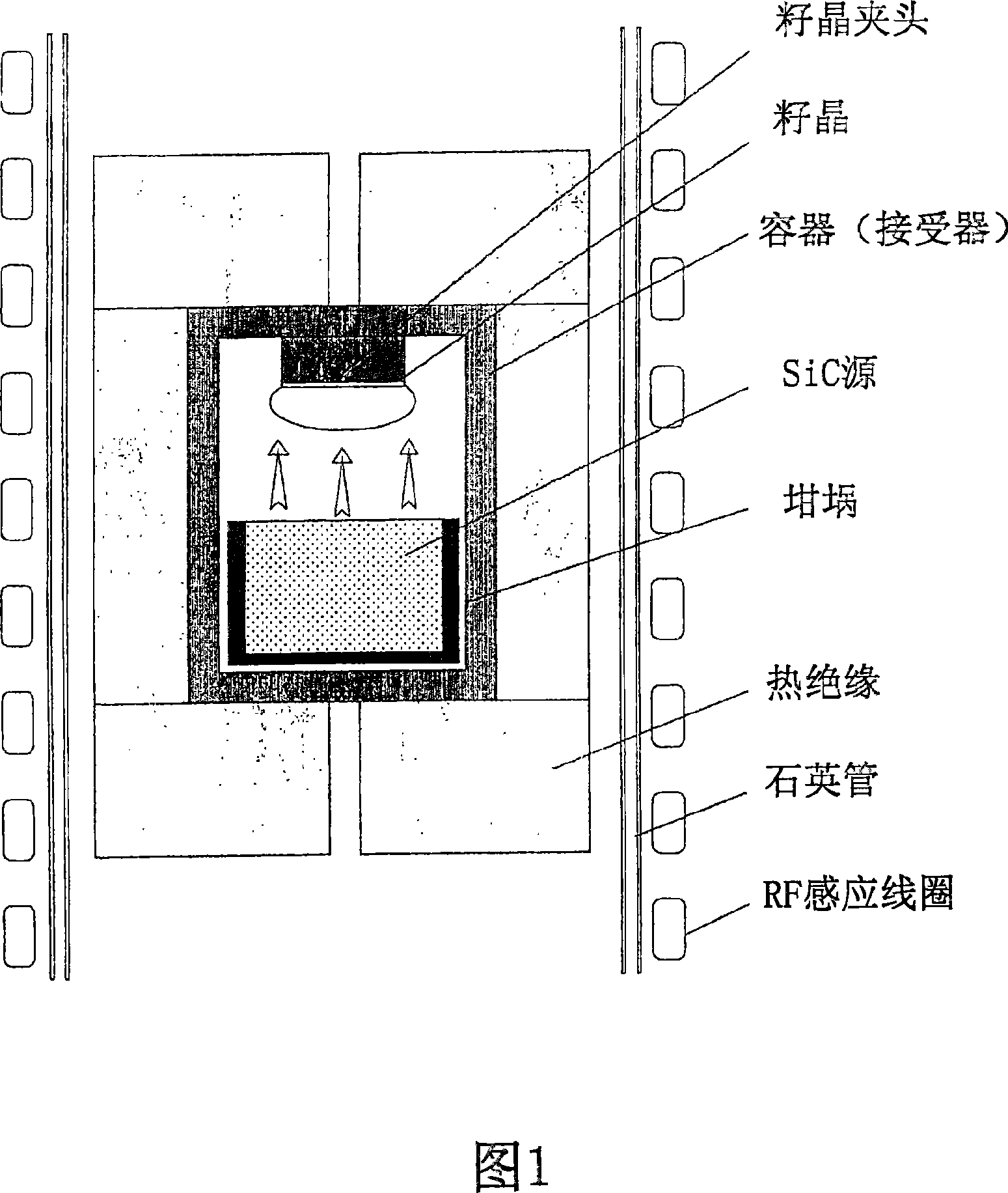
[0042] According to the present invention, vanadium-doped semi-insulating single crystal 6H SiC with high resistivity, low capacitance and high thermal conductivity is fabricated using physical vapor transport (PVT) growth technique. A schematic diagram of the PVT growth assembly is given in Figure 1. The growth vessel and other parts of the hot zone are made of dense graphite and purified using well-described industrial procedures to reduce the boron content, preferably below 0.05 ppm by weight. The impurity content generally in low boron graphite is shown in Table 1.

[0043] Table 1 Graphite purity used for SiC crystal growth, GDMS, wppm.

[0044] B

Na

Al

Si

S

Cl

Ti

V

Fe

Ni

0.03

<0.01

<0.05

0.16

0.66

<0.05

<0.01

<0.005

<0.01

<0.01

[0045] High purity polycrystalline SiC is synthesized in a separate process and used as a source in the PVT growth process. Metallic impuri...

example 1

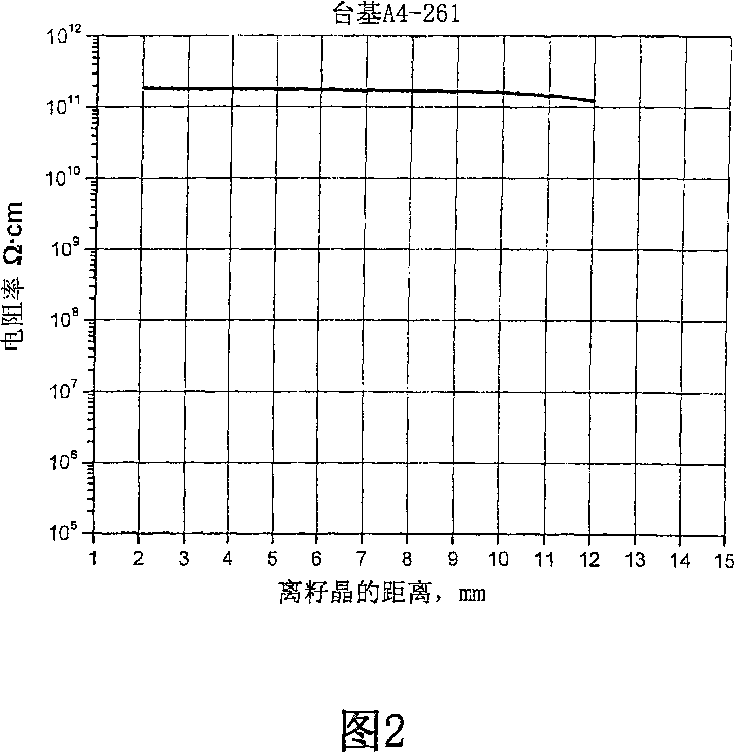
[0054] A 2 inch diameter vanadium-doped semi-insulating SiC crystal (boule A4-261) was grown at a seed temperature of 2050°C and a source temperature of 2100°C. The growth environment was 10 Torr helium. The obtained crystals showed that at 10 11 Very high and uniform resistivity above ohm-cm, as shown in Figure 2, with a standard deviation of about 3.5% over the substrate area. Substrate capacitance measured by mercury probe at 10kHz at 0.2 pF / mm 2 the following.

[0055] The impurity content of crystal A4-261 was analyzed by secondary ion mass spectrometry (SIMS). The results are shown in Table 3.

[0056] Table 3 Impurity content in SI SiC crystal A4-261, cm -3

[0057]

B

N

V

Al

Ti

2.3·10 16

4.9·10 16

6.0·10 16

3.0·10 14

4.0·10 14

[0058] The vanadium content is close to an order of magnitude lower than its solubility in SiC, but at the same time is...

example 2

[0061] The 2 inch diameter dopant Semi-insulating SiC crystals of vanadium (Mesa A1-367).

[0062] The impurity content of mesa A4-367 has been analyzed by SIMS and the results are shown in Table 4.

[0063] Table 4 Impurity content in SI SiC crystal A1-367, cm -3

[0064] B

N

V

Al

Ti

4.3·10 16

9·10 15

5.3·10 16

3.0·10 14

2.0·10 14

[0065] SIMS data show that the nitrogen content is reduced to a level below the boron content. It can also be seen that, similar to Example 1, the vanadium content is substantially below its solubility and sufficiently high above the net shallow impurity concentration (boron minus nitrogen) to obtain semi-insulating properties, as described below.

[0066] Sufficient vanadium doping in combination with relatively low-level nitrogen leads to very high crystal resistivity. In fact, the resistivity is higher than the upper sensitivity limit of ...


PUM


Abstract

The invention relates to substrates of semi-insulating silicon carbide used for semiconductor devices and a method for making the same. The substrates have a resistivity above 106 Ohm-cm, and preferably above 108 Ohm-cm, and most preferably above 109 Ohm-cm, and a capacitance below 5 pF / mm2 and preferably below 1 pF / mm2. The electrical properties of the substrates are controlled by a small amount of added deep level impurity, large enough in concentration to dominate the electrical behavior, but small enough to avoid structural defects. The substrates have concentrations of unintentional background impurities, including shallow donors and acceptors, purposely reduced to below 5 DEG 1016 cm-3, and preferably to below 1 DEG 1016 cm-3, and the concentration of deep level impurity is higher, and preferably at least two times higher, than the difference between the concentrations of shallow acceptors and shallow donors. The deep level impurity comprises one of selected metals from the periodic groups IB, IIB, IIIB, IVB, VB, VIB, VIIB and VIIIB. Vanadium is a preferred deep level element. In addition to controlling the resistivity and capacitance, a further advantage of the invention is an increase in electrical uniformity over the entire crystal and reduction in the densityof crystal defects.

Description

technical field [0001] The present invention relates to the production of semi-insulating SiC material, and the growth of high quality wafers of this material to fabricate substrates useful for RF, microwave and other device applications. Background technique [0002] Silicon carbide (SiC) is a wide bandgap semiconductor material with a unique combination of electrical and thermophysical properties that make it extremely attractive for use in new generations of electronic devices. These properties include high breakdown field strength, high practical operating temperature, high electron saturation velocity, high thermal conductivity, and radiation hardness. These properties enable devices to operate at considerably higher powers, at higher temperatures, and with greater radiation resistance than comparable devices made from more conventional semiconductors such as Si and GaAs (D.L. Barrett et al., J. Crystal Growth, pp. 109, 1991, pp. 17-23). Transistors fabricated from hi...

Claims


Application Information

Patent Timeline
Patent Type & Authority Applications(China)
IPC IPC(8): C30B25/12
CPCC30B23/00H01L21/02529H01L29/1608C30B29/36H01L21/2033H01L21/02631H01L21/02378H01L21/02581
Inventor 陈继宏伊利娅·茨维巴克阿维那希·K·古普塔多诺万·L·巴雷特理查德·H·霍普金斯爱德华·塞默纳斯托马斯·A·安德森安德鲁斯·E·苏齐斯
Owner II VI
Learn More