Ink composition for light sintering, wiring board using same and manufacturing method therefor

a technology of light sintering and composition, which is applied in the direction of conductive pattern formation, conductive material removal by irradiation, transportation and packaging, etc., can solve the problems of many limitations in selecting a wiring board or an ink, insufficient adhesion, and inability to reduce the fabrication cost of resultant wiring boards, so as to reduce the production cost of a wiring board, and shorten the process time

Active Publication Date: 2018-10-02
KOREA ELECTRONICS TECH INST
View PDF28 Cites 4 Cited by
  • Summary
  • Abstract
  • Description
  • Claims
  • Application Information

AI Technical Summary

Benefits of technology

[0045]In accordance with the present invention, when a wiring pattern of a wiring board is formed using cheap copper nanoparticles having copper oxide films (hereinafter referred to as “copper oxide nanoparticles”) as a raw material of a conductive ink, production cost of the wiring board may be reduced. That is, since a wiring pattern of a wiring board can be formed using a conductive ink including copper oxide nanoparticles, which are cheaper than pure copper nanoparticles, production cost of a wiring board may be reduced.
[0046]In addition, upon sintering after printing the conductive ink including the copper oxide nanoparticles on a wiring board, copper oxide films formed on surfaces of the copper nanoparticles may be removed by performing short-wavelength light irradiation instead of thermal sintering. Accordingly, process time may be shortened and damage of the wiring board may be prevented by a sintering process through the short-wavelength light irradiation. Here, the copper oxide nanoparticles are in an insulation state before the light sintering, but are reduced into pure copper nanoparticles by the light sintering, thereby forming a wiring pattern made of copper having electrical conductivity.
[0047]Accordingly, by applying the conductive ink according to the present invention to a board body of a flexible printed circuit board used in a digitizer, a wiring pattern may be formed without damaging the board body.
[0048]In addition, when a wiring pattern is formed on a wiring board using the conductive ink including the copper nanoparticles having copper oxide films, the wiring pattern may be formed to have a high aspect ratio by screen-printing. That is, since a signal transmission speed of a wiring board depends upon resistance, the wiring pattern may be formed to have a high aspect ratio by screen-printing.
[0049]Meanwhile, in the present invention, since a wiring pattern of a wiring board may be formed using an ink composition including pure copper particles and copper oxide nanoparticles, which are cheaper than a silver material, production cost of a wiring board may be reduced.
[0050]Since the ink composition according to the present invention includes pure copper particles, compactness of a wiring pattern may be improved compared to the case in which copper oxide nanoparticles are used alone. That is, a wiring pattern is formed in a shape wherein a plurality of pores are contained therein due to gas generated upon light sintering of an ink composition including only copper oxide nanoparticles as copper particles. On the other hand, when pure copper particles are included as in the present invention, the amount of gas generated in a light sintering process is reduced and thus the amount of pores present in the interior of a wiring pattern may be reduced, whereby a wiring pattern having increased compactness may be formed.

Problems solved by technology

However, silver included in conductive inks is very expensive and thus, when wiring patterns are formed using the conductive inks, there is limitation in reducing fabrication costs of resultant wiring boards.
In addition, since a thermal sintering process is required, there are many limitations in selecting a wiring board or an ink.
Further, when wiring patterns are formed using a silver ink or a silver paste, problems such as flaking, insufficient adhesion, and high resistance of a wiring pattern formed after thermal sintering are encountered.

Method used


Image

  • Ink composition for light sintering, wiring board using same and manufacturing method therefor
  • Ink composition for light sintering, wiring board using same and manufacturing method therefor
  • Ink composition for light sintering, wiring board using same and manufacturing method therefor

Examples


first example

[0074]An ink composition for light sintering according to a first example includes copper oxide nanoparticles having copper oxide films, a reducing agent for reducing copper oxidized by light irradiation to form copper nanoparticles, a dispersing agent, a binder, and a solvent.

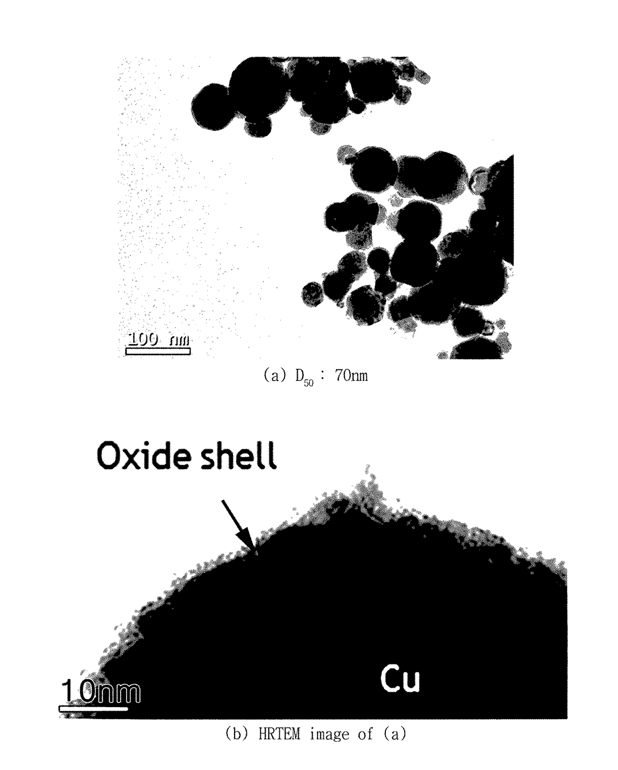
[0075]Although copper oxide nanoparticles are nonconductors, the copper oxide nanoparticles are converted into pure copper nanoparticles having electrical conductivity by light irradiation, thus being used as a source of a conductor. The copper oxide nanoparticles are core-shell type particles, may have a structure wherein a copper oxide film is formed so as to have a thickness of 500 nm or less on surfaces of copper nanoparticles, and may have a particles size of less than 1 μm. With regard to this, when the copper oxide film is coated so as to have a thickness of greater than 500 nm, a portion of the copper oxide film might not be reduced into copper by light irradiation. Accordingly, the copper oxide nanopa...

second example

[0140]An ink composition for light sintering according to a second example includes silver oxide and copper oxide nanoparticles having copper oxide films and may further include a reducing agent for reducing copper oxidized by light irradiation to form copper nanoparticles, a dispersing agent, a binder, and a solvent.

[0141]The silver oxide is silver oxide (I) or silver oxide (II). Here, the silver oxide (I) is Ag2O which is dark brown to blackish brown, has a specific gravity of 7.22, and is degradable at about 160° C. The silver oxide (II) is AgO which is charcoal gray, has a specific gravity of 7.483, and is degradable at about 100° C.

[0142]When xenon white light is irradiated to such silver oxide, optical absorption may be easily performed due to the color, i.e., brown or black, of the silver oxide. In addition, decomposition may be easily performed and thus sintering may be easily performed. Further, a denser wiring pattern may be fabricated. Hereinafter, a light sintering proce...

third example

[0212]An ink composition for light sintering according to a third example includes pure copper particles and copper oxide nanoparticles having copper oxide films and may further include a reducing agent for reducing copper oxidized by light irradiation to form copper nanoparticles, a dispersing agent, a binder, and a solvent.

[0213]The pure copper particles may be spherical particles having a size (D50) of 2 μm or less or plate-shaped particles having a size (D50) 4 μm or less. When the pure copper particles are plate-shaped particles, the pure copper particles may have a flake or multi-angle plate shape. For example, FIG. 13 illustrates an SEM image of pure copper particles having a D50 of 880 nm.

[0214]The pure copper particles have an oxidation resistant film on the exteriors thereof to prevent oxidation. As the oxidation resistant film, fatty acid, such as steric acid, may be used. The oxidation resistant film may be formed to a thickness of several nanometers on the exteriors of ...


PUM

PropertyMeasurementUnit
particles sizeaaaaaaaaaa
thicknessaaaaaaaaaa
sizeaaaaaaaaaa

Abstract

The present invention relates to an ink composition for light sintering, a wiring board using the same, and a method of fabricating the wiring board. The present invention aims to provide formation of a wiring pattern without damage to thin and soft wiring boards such as a flexible printed circuit board. The present invention provides an ink composition for light sintering including copper oxide nanoparticles having copper oxide films, a reducing agent for reducing copper oxidized by light irradiation to form copper nanoparticles, a dispersing agent, a binder, and a solvent.

Description

CROSS REFERENCE TO RELATED APPLICATIONS[0001]Any and all priority claims identified in the Application Data Sheet, or any correction thereto, are hereby incorporated by reference under 37 CFR 1.57. For example, this application is a U.S. National Phase of International Application No. PCT / KR2015 / 003226, filed on Apr. 1, 2015 and published on Oct. 8, 2015 as WO 2015 / 152625. PCT / KR2015 / 003226 claims priority to and the benefit of Korean Patent Application No. 10-2014-0038579 filed on Apr. 1, 2014, Korean Patent Application No. 10-2014-0186689 filed on Dec. 23, 2014 and Korean Patent Application No. 10-2014-0186691 filed on Dec. 23, 2014, each of which is hereby incorporated by reference in their entireties.TECHNICAL FIELD[0002]The present invention relates to an ink composition, a wiring board using the same, and a method of fabricating the wiring board using the ink composition, and more particularly, to an ink composition for light sintering including copper nanoparticles having cop...

Claims


Application Information

Patent Timeline
Patent Type & Authority Patents(United States)
IPC IPC(8): H01B1/22C09D11/037H05K3/02B22F1/02B22F1/00H05K3/12H05K3/22C09D11/00H05K1/09C09D11/52B22F1/0545B22F1/107B22F1/16
CPCH05K1/095B22F1/0022B22F1/0074B22F1/02C09D11/037C09D11/52H05K1/097H05K3/027H05K3/1216H05K3/227H01B1/22H05K2201/032B22F2301/10B22F2302/25B22F9/24H01B1/20B22F1/107B22F1/16B22F1/0545
Inventor KIM, YOONJINCHO, JINWOOSHIN, KWONWOOSEO, YONGGONKIM, YEONWONJANG, SANGHYEONJO, NAMJE
Owner KOREA ELECTRONICS TECH INST
Why Eureka
Try Eureka