

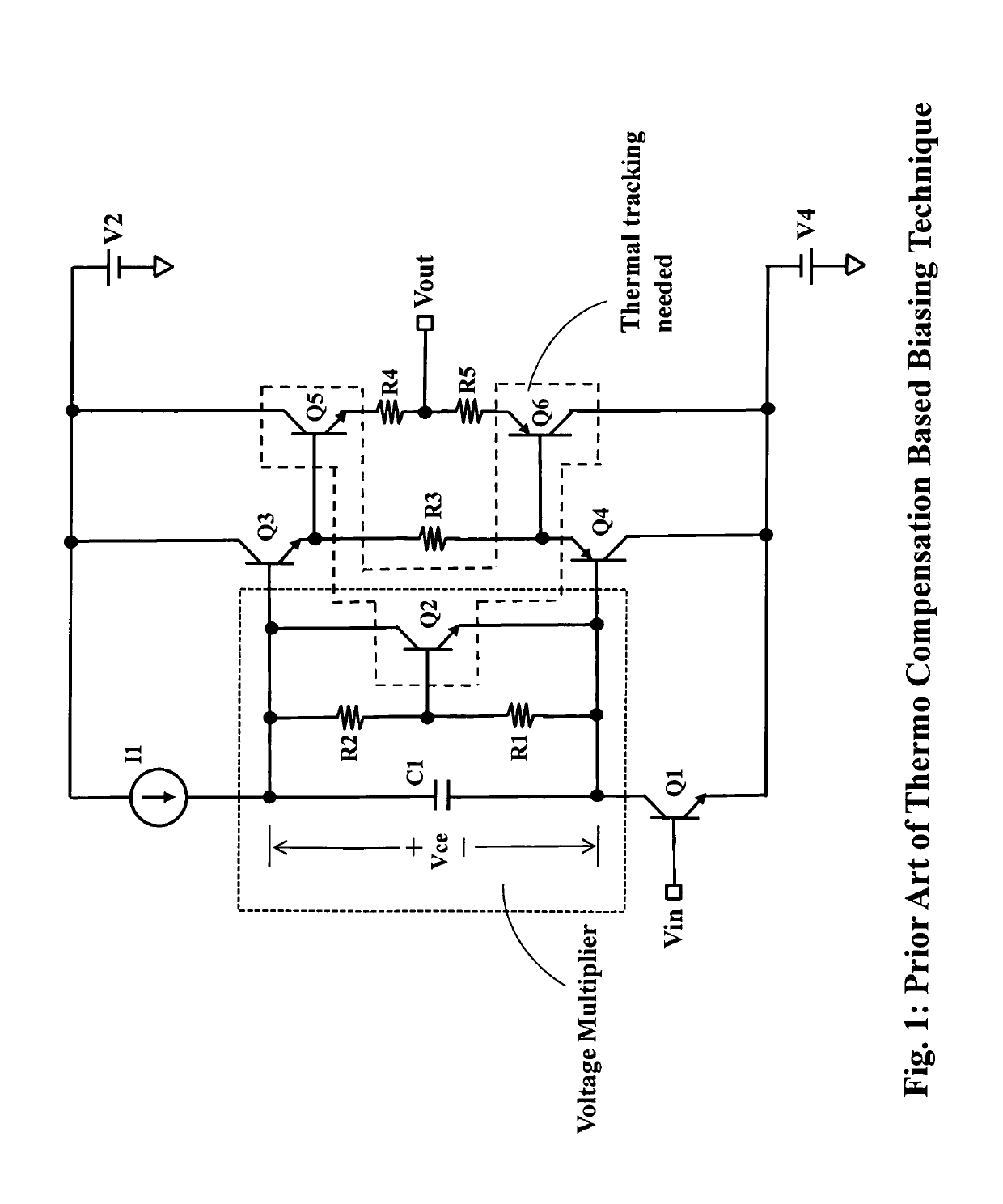
Biasing method without using thermal compensation applicable for both class-A and class-AB audio power amplifier
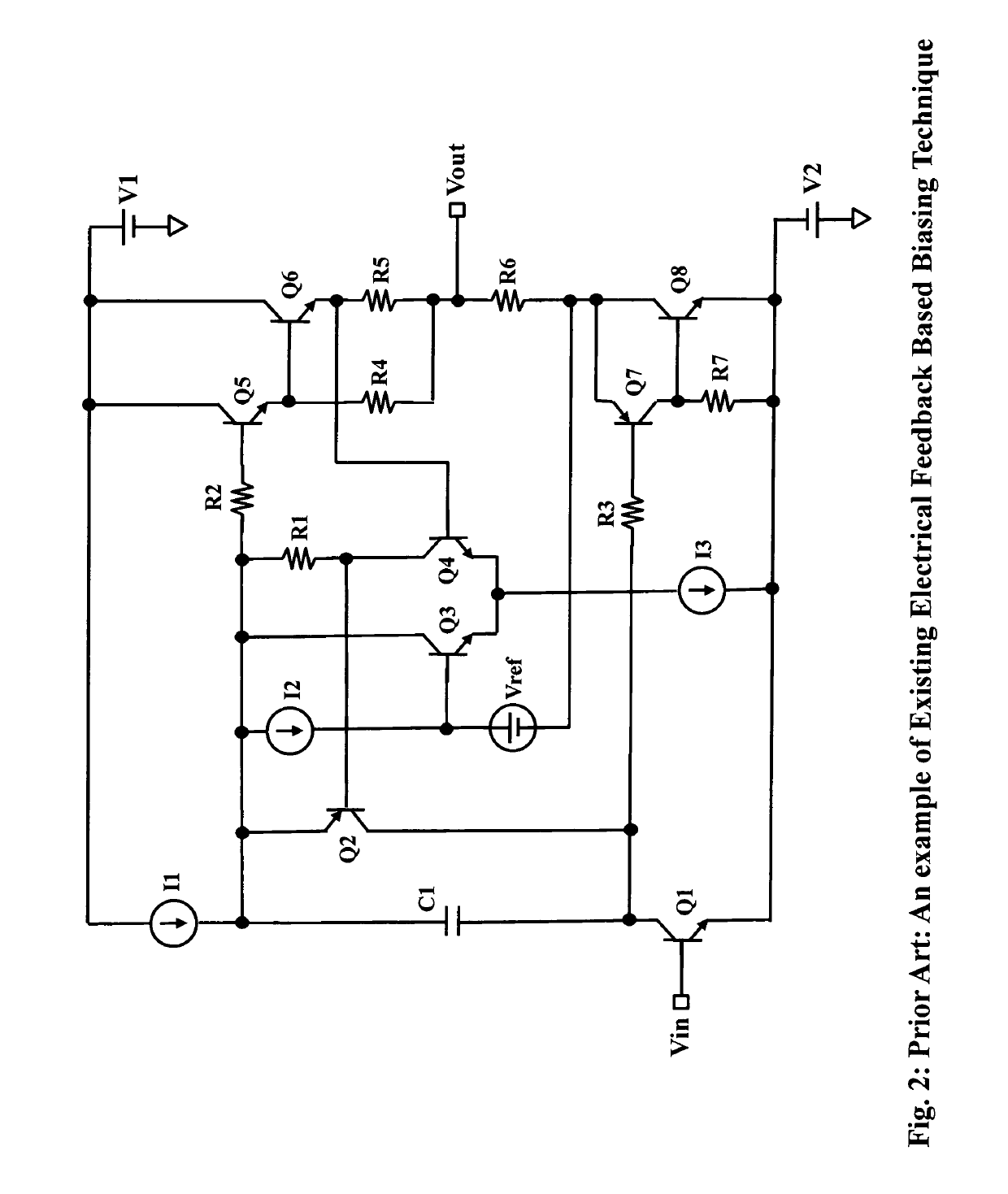
a technology of audio power amplifier and thermal compensation, applied in the direction of amplifiers with diodes, amplifiers with semiconductor devices/discharge tubes, amplifiers with diodes, etc., can solve the problems of thermal-electrical compensation conditions that are difficult (if not impossible) to achieve, performance variation including distortion behavior changes and reliability deterioration, and difficulty in accurate and reliable biasing, etc.
- Summary
- Abstract
- Description
- Claims
- Application Information
AI Technical Summary
Benefits of technology
Problems solved by technology
Method used
Image

Examples
Embodiment Construction
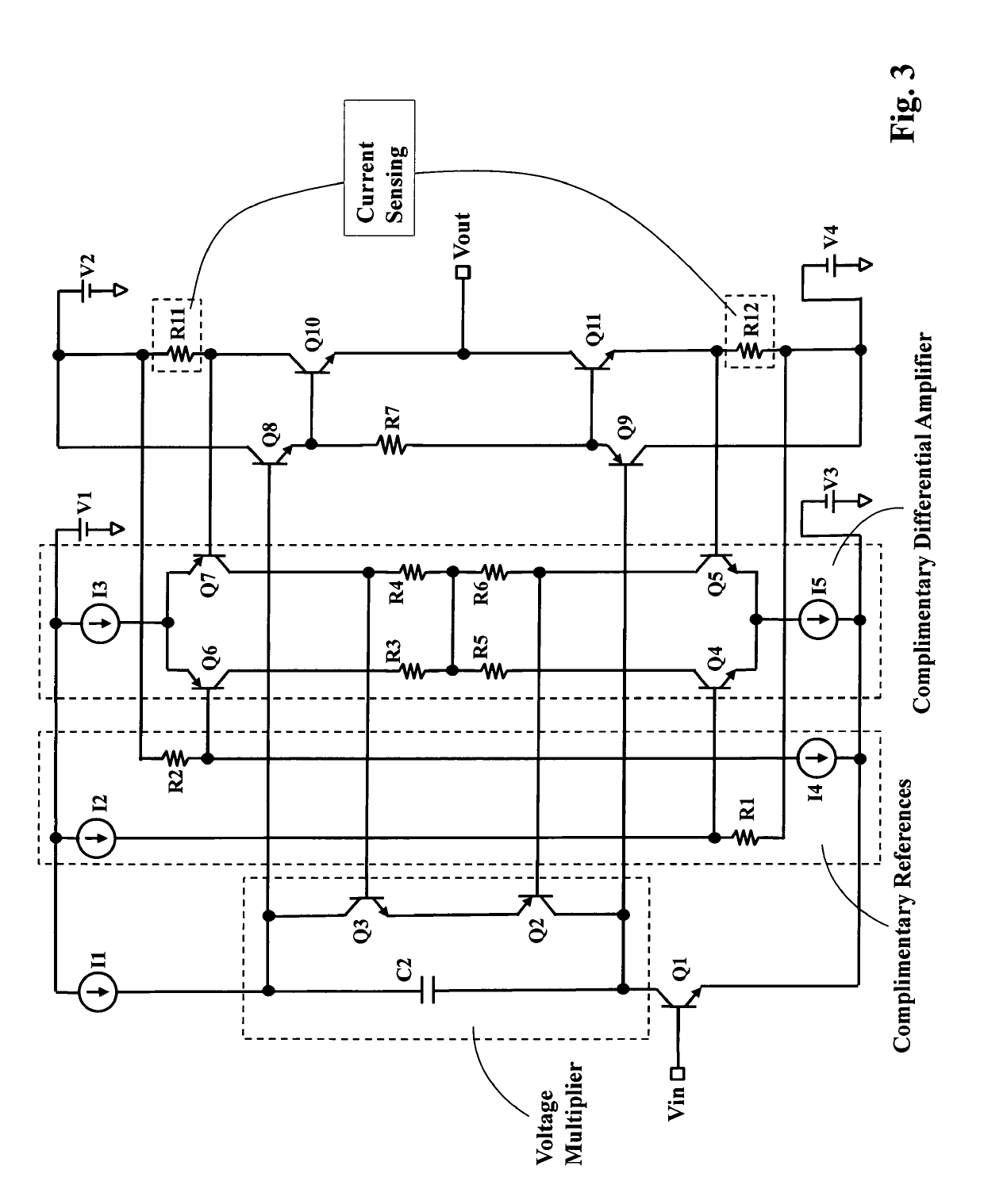
[0021]An implementation example of the proposed new biasing technique is shown in FIG. 3. The core biasing scheme is comprised of four sub functional circuits: a complimentary output power device current sensing circuit which generates current corresponding voltage outputs and is comprised of R11 and R12; a complimentary differential amplifier which takes the outputs of the current sensing circuit as it's inputs against a complimentary reference voltage pair and is comprised of Q4˜Q7, I3, I5, and R3˜R6; a complimentary reference generator which creates aforementioned reference voltages for the previously described complimentary differential amplifier and is comprised of I2, I4, R1 and R2; a voltage multiplier which takes the amplified voltage output of the complimentary differential amplifier as it's input and generates the final output voltage to be used as the bias voltage for the output stage and is comprised of Q2, Q3 and C2.
[0022]The key uniqueness of the new design is that the...
PUM
 Abstract
Description
Claims
Application Information