
Organic compound and organic electroluminescence device using the same

a technology of organic compounds and electroluminescent devices, which is applied in the direction of organic chemistry, luminescent compositions, and group 5/15 element organic compounds, can solve the problems of unsatisfactory half-life time, power consumption, luminance, efficiency, etc., and achieves improved deep blue emission, longer half-life time, and high luminance and current efficiency

Active Publication Date: 2019-10-22
LUMINESCENCE TECH
View PDF2 Cites 1 Cited by
  • Summary
  • Abstract
  • Description
  • Claims
  • Application Information

AI Technical Summary

Benefits of technology

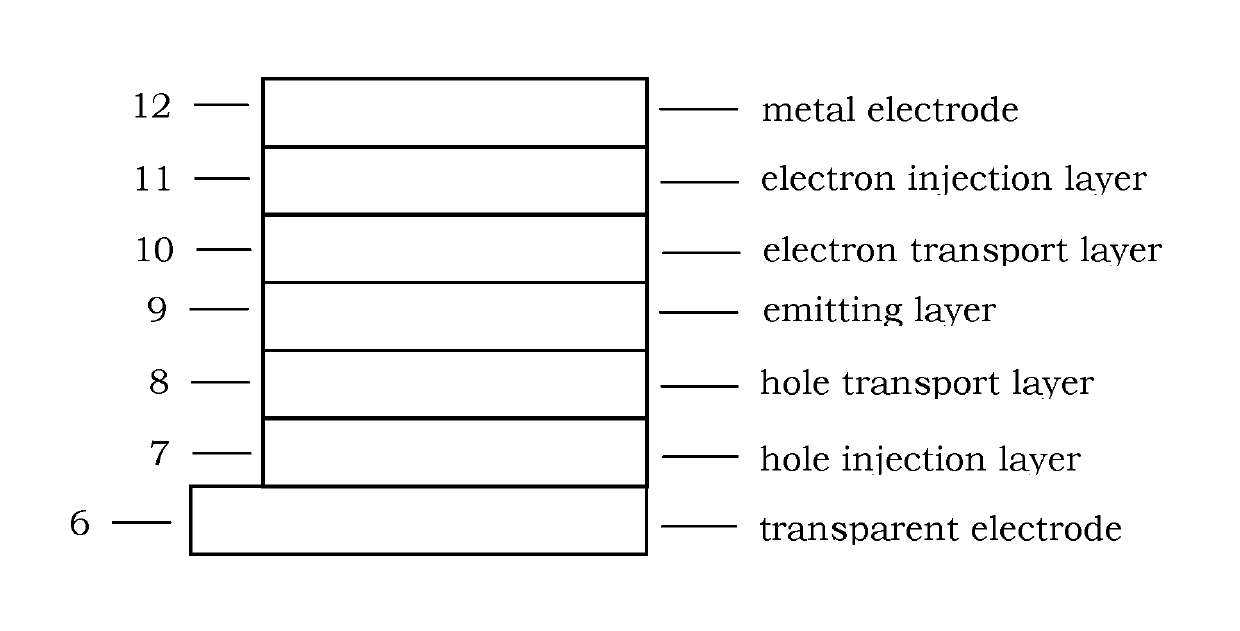
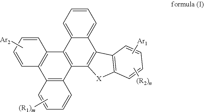
The invention provides a new organic compound that can be used in organic EL devices. It has higher luminance, current efficiency, longer half-life time, and improved deep blue emission. The compound can also operate under reduced voltage and exhibit higher current efficiency and longer half-life time. Additionally, it can be used as a phosphorescent host material, fluorescent host material, or fluorescent dopant material in the emitting layer, or an electron transporting material in an organic EL device to improve power consumption, luminance, current efficiency, device color, or life time.

Problems solved by technology

For full-colored flat panel displays using organic EL devices, the organic materials used in the organic EL devices are still unsatisfactory in half-life time, power consumption, luminance, and efficiency.

Method used


Image

  • Organic compound and organic electroluminescence device using the same
  • Organic compound and organic electroluminescence device using the same
  • Organic compound and organic electroluminescence device using the same

Examples


example 1

Synthesis of Intermediate A

[0026]

[0027]A mixture of 3 g (8.4 mmol) of 10-bromobenzo[g]chrysene (synthesis reference: US 20100327266), 2.5 g (10.1 mmol) of 4,4,4′,4′,5,5,5′,5′-octamethyl-2,2′-bi(1,3,2-dioxaborolane), 0.12 g (0.1 mmol) of Pd(PPh3)4, 1.0 g (12.6 mmol) of sodium acetate, and 60 ml of 1,4-dioxane was degassed and placed under nitrogen, and then heated at 100° C. for 6 hrs. After the reaction finished, the mixture was allowed to cool to room temperature. Subsequently, the organic layer was extracted with ethyl acetate and water, and then dried with anhydrous magnesium sulfate. After the solvent was removed, the residue was purified by column chromatography on silica to give Intermediate A (2.8 g, 85%).

Synthesis of Intermediate B

[0028]

[0029]A mixture of 2 g (5.0 mmol) of Intermediate A, 1.7 g (5.0 mmol) of methyl 5-bromo-2-iodobenzoate, 0.06 g (0.05 mmol) of Pd(PPh3)4, 10 ml of 2M Na2CO3(aq), 10 ml of EtOH, and 30 ml of toluene was degassed and placed under nitrogen, and t...

example 2

Synthesis of Compound C15

[0042]

[0043]A mixture of 3 g (6.3 mmol) of Intermediate C, 2.1 g (9.4 mmol) of anthracen-9-ylboronic acid, 0.07 g (0.06 mmol) of Pd(PPh3)4, 13 ml of 2M Na2CO3(aq), 30 ml of EtOH, and 90 ml of toluene was degassed and placed under nitrogen, and then heated at 100° C. for 12 hrs. After the reaction finished, the mixture was allowed to cool to room temperature, and then filtered to give compound C15 (3.1 g, 88%). MS (m / z, FAB+): 571.5.

example 3

Synthesis of Compound C29

[0044]

[0045]A mixture of 1 g (1.9 mmol) of Intermediate G, 1.1 g (4.4 mmol) of 2-chloro-4,6-diphenyl-1,3,5-triazine, 0.01 g (0.01 mmol) of Pd(PPh3)4, 4 ml of 2M Na2CO3(aq), 10 ml of EtOH, and 30 ml of toluene was degassed and placed under nitrogen, and then heated at 100° C. for 12 hrs. After the reaction finished, the mixture was allowed to cool to room temperature. Subsequently, the organic layer was extracted with dichloromethane and water, and then dried with anhydrous MgSO4. After the solvent was removed, the residue was purified by column chromatography on silica to give compound C29 (0.6 g, 53%). MS (m / z, FAB+): 626.5.


PUM

PropertyMeasurementUnit
EQEaaaaaaaaaa
EQEaaaaaaaaaa
internal quantum efficiencyaaaaaaaaaa

Abstract

An organic compound which can be used as the phosphorescent host material, the fluorescent host material, or the fluorescent dopant material of the light emitting layer, and / or the electron transporting material in the organic electroluminescence device is disclosed. The organic electroluminescence device employing the organic compound can lower driving voltage, prolong half-lifetime, and increase current efficiency.

Description

FIELD OF INVENTION[0001]The present invention relates to a novel organic compound and, more particularly, to an organic electroluminescence device using the organic compound.BACKGROUND OF THE INVENTION[0002]An organic electroluminescence (organic EL) device is an organic light-emitting diode (OLED) in which the light emitting layer is a film made from organic compounds, which emits light in response to the electric current. The light emitting layer containing the organic compound is sandwiched between two electrodes. The organic EL device is applied to flat panel displays due to its high illumination, low weight, ultra-thin profile, self-illumination without back light, low power consumption, wide viewing angle, high contrast, simple fabrication methods and rapid response time.[0003]Typically, the organic EL device is composed of organic material layers sandwiched between two electrodes. The organic material layers include, e.g., hole injection layer (HIL), hole transporting layer (...

Claims


Application Information

Patent Timeline
Patent Type & Authority Patents(United States)
IPC IPC(8): H01L51/50C07D333/76C09K11/06C07C13/62C07F7/08H01L51/00C07D209/82C07D307/91H10K99/00
CPCH01L51/0073H01L51/5016C07C13/62H01L51/5072C07D333/76C09K11/06C07D307/91C07D209/82H01L51/0058C07F7/0816H01L51/0072H01L51/0074C09K2211/1088C09K2211/1011C09K2211/1029C09K2211/1092C09K2211/1096C07C211/61C07D307/77C07D333/50C07D405/04C07D405/14C07D409/04C07D413/10C07D471/04C07D409/14C07D519/00C07D401/14C07D401/10C07D403/14C07D403/10C07D239/26C07D251/24C07D209/86C07D209/80C07D219/02C07D213/16C07D265/38C07D279/22C07C15/38C07C15/28C07C15/30C07C15/24C07C13/66C07F9/5325C09K2211/1007C09K2211/1014C09K2211/1033C09K2211/1037C09K2211/1044C09K2211/1059H10K85/622H10K85/626H10K85/649H10K85/657H10K85/6572H10K85/6574H10K85/6576H10K85/40H10K50/11C07C2601/10H10K85/624H10K85/636H10K85/633H10K2101/10H10K50/16
Inventor YEN, FENG-WENTENG, CHIN-MIN
Owner LUMINESCENCE TECH
Learn More