Systems and methods for combined x-ray reflectometry and photoelectron spectroscopy

a technology of photoelectron spectroscopy and reflectometry, applied in the field of xray metrology systems and methods, can solve the problems of limited information concerning the composition and shape of nanostructure materials, difficult characterization, limited characterization, etc., and achieves improved measurement accuracy, improved throughput and measurement accuracy, and improved measurement performance

Active Publication Date: 2021-01-19
KLA CORP
View PDF37 Cites 8 Cited by
  • Summary
  • Abstract
  • Description
  • Claims
  • Application Information

AI Technical Summary

Benefits of technology

[0016]In one aspect, a combined XRR and XPS system includes an x-ray illumination source and x-ray illumination optics shared by both the XRR and XPS measurement subsystems. A combined XRR and XPS system increases throughput and measurement accuracy by illuminating the same area of the wafer and collecting XRR and XPS measurement data simultaneously.
[0017]In general, a combined XRR and XPS system improves measurement accuracy by employing XRR measurement data to improve measurements performed by the XPS subsystem, and vice-versa. In some embodiments, a combined XRR and XPS system illuminates the same target simultaneously. In addition, a combined XRR and XPS system enables simultaneous analysis of both XRR and XPS measurement data to more accurately estimate values of one of more parameters of interest. Simultaneous XRR and XPS measurements of a metrology target by a combined XRR and XPS system increases measurement throughput compared to separate measurements of the metrology target by separate XRR and XPS systems. Furthermore, simultaneous XRR and XPS measurements of a metrology target by a combined XRR and XPS system avoid target positioning errors that occur when separate measurements of the metrology target are performed by separate XRR and XPS systems.
[0018]In some embodiments, the XRR measurement subsystem is configured as a grazing incidence, small angle x-ray scatterometry (GI-SAXS) system operating near the critical angles for reflection for semiconductor materials. In some other embodiments, the XRR measurement subsystem is configured as a reflective, small-angle x-ray scatterometer (RSAXS). In some embodiments, the RSAXS measurements are performed with x-ray radiation in the soft x-ray (SXR) region (i.e., 80-3000 eV) at grazing angles of incidence in the range of 5-20 degrees. These relatively large grazing angles enable deeper penetration into structures under measurement and smaller measurement spot size (e.g., less than 50 micrometers). In some embodiments, RSAXS measurements of a semiconductor wafer are performed over a range of wavelengths, angles of incidence, and azimuth angles with a small beam spot size.
[0019]In one aspect, the source area of the x-ray illumination source is characterized by a lateral dimension of less than 20 micrometers. In some embodiments, the source area is characterized by a lateral dimension of 10 micrometers or less. Small source size enables illumination of a small target area on the specimen with high brightness, thus improving measurement precision, accuracy, and throughput.
[0023]In yet another aspect, the precision and accuracy of parameters measured with either or both XRR and XPS techniques is improved by identifying shared model parameters that are mathematically resolved using data sets derived from XRR and XPS measurements either sequentially or in parallel.

Problems solved by technology

As devices (e.g., logic and memory devices) move toward smaller nanometer-scale dimensions, characterization becomes more difficult.
Devices incorporating complex three-dimensional geometry and materials with diverse physical properties contribute to characterization difficulty.
Accurate information concerning the material composition and shape of nanostructures is limited in the process development environment of a leading-edge, front-end semiconductor fabrication facility.
With limited knowledge of material composition and shape of nanostructures available apriori, measurement recipe development and validation is a slow and tedious process.
For example, cross-sectional transmission electron microscopy (TEM) images are used to guide optical scatterometry model development, but TEM imaging is slow and destructive.
Furthermore, when absorbing materials are present in the structure under measurement, penetration and scattering of illumination light in the optical region (e.g., 0.5-10 ev) limits the utility of conventional optical metrology systems.
Similarly, electron beam based metrology systems struggle to penetrate semiconductor structures due to absorption and scattering of the illuminating, backscattered, and secondary emission electrons.
Atomic force microscopes (AFM) and scanning-tunneling microscopes (STM) are able to achieve atomic resolution, but they can only probe the surface of the specimen.
In addition, AFM and STM microscopes require long scanning times that make these technologies impractical in a high volume manufacturing (HVM) setting.
Scanning electron microscopes (SEM) achieve intermediate resolution levels, but are unable to penetrate structures to sufficient depth.
Thus, high-aspect ratio holes are not characterized well.
In addition, the required charging of the specimen has an adverse effect on imaging performance.
However, scattering of hard x-rays from shallow structures, e.g., logic metrology applications, is weak, which severely limits achievable measurement resolution and throughput.
As such, T-SAXS has not been shown to be a viable option for logic metrology applications in an HVM environment.
With limited knowledge of material composition of nanostructures available apriori, measurement accuracy is limited.
Since, material geometry is not accurately known, apriori, the resulting chemical composition measurements suffer from poor accuracy.

Method used


Image

  • Systems and methods for combined x-ray reflectometry and photoelectron spectroscopy
  • Systems and methods for combined x-ray reflectometry and photoelectron spectroscopy
  • Systems and methods for combined x-ray reflectometry and photoelectron spectroscopy

Examples


Embodiment Construction

[0031]Reference will now be made in detail to background examples and some embodiments of the invention, examples of which are illustrated in the accompanying drawings.

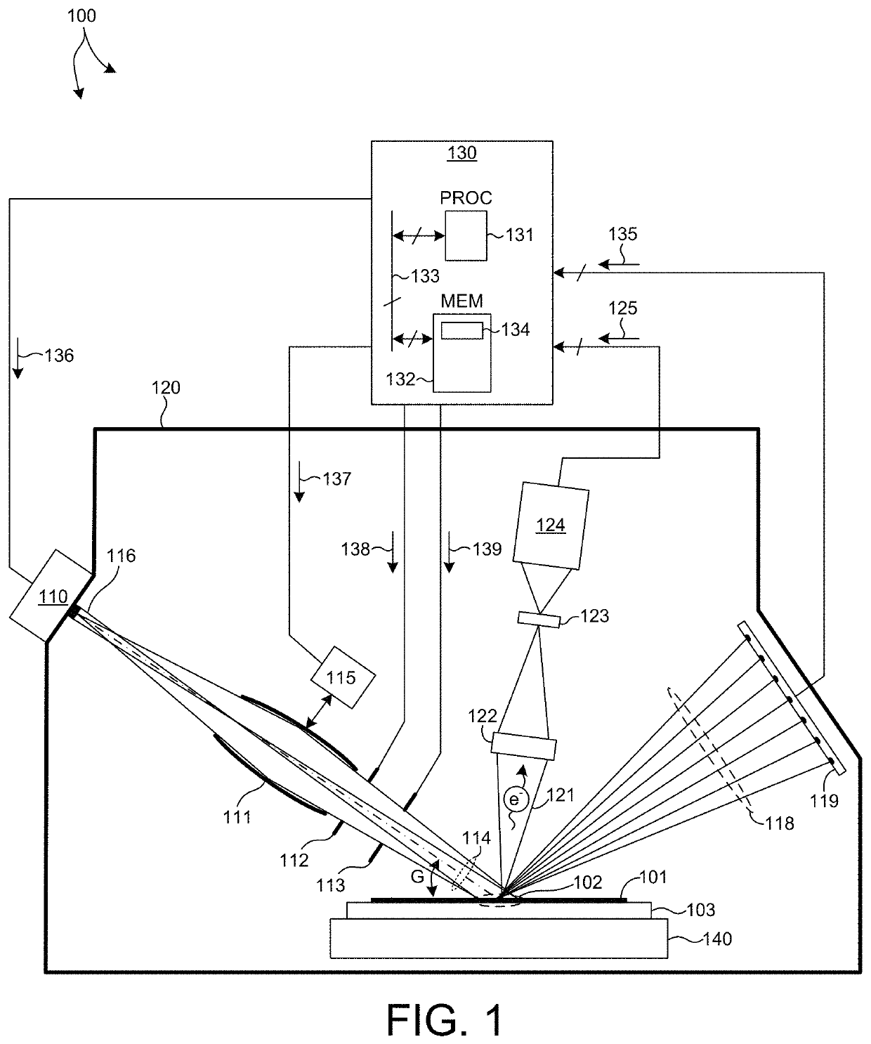
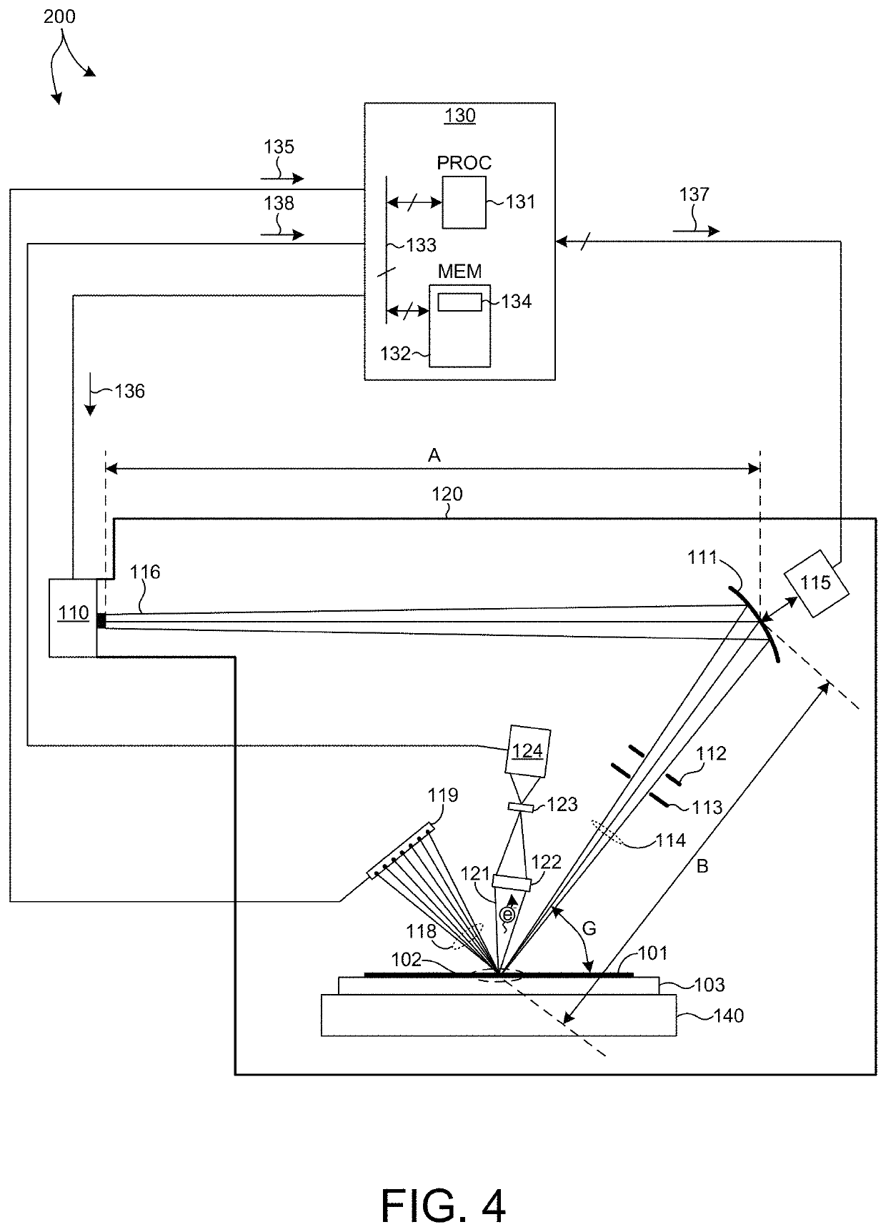
[0032]Methods and systems for measuring structural and material characteristics (e.g., material composition, dimensional characteristics of structures and films, etc.) of semiconductor structures associated with different semiconductor fabrication processes with a combined x-ray reflectometry (XRR) and x-ray photoelectron spectroscopy (XPS) measurement system are presented.

[0033]In one aspect, a combined XRR and XPS system includes an X-ray illumination source and X-ray illumination optics shared by both the XRR and XPS measurement subsystems. Sharing a common X-ray illumination source and X-ray illumination optics reduces system complexity, cost, and machine footprint in a fabrication facility. In addition, a combined XRR and XPS system increases throughput and measurement accuracy by illuminating the same area of th...


PUM

PropertyMeasurementUnit
photon energyaaaaaaaaaa
grazing incidence angleaaaaaaaaaa

Abstract

Methods and systems for measuring structural and material characteristics of semiconductor structures based on combined x-ray reflectometry (XRR) and x-ray photoelectron spectroscopy (XPS) are presented herein. A combined XRR and XPS system includes an x-ray illumination source and x-ray illumination optics shared by both the XRR and XPS measurement subsystems. This increases throughput and measurement accuracy by simultaneously collecting XRR and XPS measurement data from the same area of the wafer. A combined XRR and XPS system improves measurement accuracy by employing XRR measurement data to improve measurements performed by the XPS subsystem, and vice-versa. In addition, a combined XRR and XPS system enables simultaneous analysis of both XRR and XPS measurement data to more accurately estimate values of one of more parameters of interest. In a further aspect, any of measurement spot size, photon flux, beam shape, beam diameter, and illumination energy are independently controlled.

Description

CROSS REFERENCE TO RELATED APPLICATION[0001]The present application for patent claims priority under 35 U.S.C. § 119 from U.S. provisional patent application Ser. No. 62 / 614,399, filed Jan. 6, 2018, the subject matter of which is incorporated herein by reference in its entirety.TECHNICAL FIELD[0002]The described embodiments relate to x-ray metrology systems and methods, and more particularly to methods and systems for improved measurement accuracy.BACKGROUND INFORMATION[0003]Semiconductor devices such as logic and memory devices are typically fabricated by a sequence of processing steps applied to a specimen. The various features and multiple structural levels of the semiconductor devices are formed by these processing steps. For example, lithography among others is one semiconductor fabrication process that involves generating a pattern on a semiconductor wafer. Additional examples of semiconductor fabrication processes include, but are not limited to, chemical-mechanical polishing...

Claims


Application Information

Patent Timeline
Patent Type & Authority Patents(United States)
IPC IPC(8): G01N23/223G01N23/2273G01N23/083G01N23/207G02B27/09H05G1/30
CPCG01N23/223G01N23/083G01N23/2076G01N23/2273G02B27/0977H05G1/30G01N23/20008G01N21/27G01B15/02G01B15/08G01J3/50G01B2210/56
Inventor SHCHEGROV, ANDREI V.KUZNETSOV, ALEXANDERKHODYKIN, OLEG
Owner KLA CORP
Why Eureka
Try Eureka