
Plasma & reactive ion etching to prepare ohmic contacts

a technology of reactive ion etching and ohmic contacts, which is applied in the direction of sustainable manufacturing/processing, final product manufacturing, vacuum evaporation coating, etc., can solve the problems of low carrier mobility, high material cost, and difficulty in settling single crystalline materials

Inactive Publication Date: 2001-06-14
ALLIANCE FOR SUSTAINABLE ENERGY
View PDF0 Cites 3 Cited by
  • Summary
  • Abstract
  • Description
  • Claims
  • Application Information

AI Technical Summary

Benefits of technology

[0005] A typical single-junction photovoltaic cell is comprised of a substrate on which to form the device, two ohmic contacts to conduct current to an external electrical circuit, and two or more semiconductor layers in series to form the semiconductor junction. At least one of these semiconductor layers (the absorber) is chosen so that its bandgap is of a value for near-optimum conversion of solar radiation. In a typical design, one semiconductor layer is doped n-type, and the adjacent layer is doped p-type. The intimate proximity of these layers forms a semiconductor p-n junction. The p-n junction provides an electric field that facilitates charge separation in the absorber layer(s) when the cell is illuminated, and charge collection at the ohmic contacts.
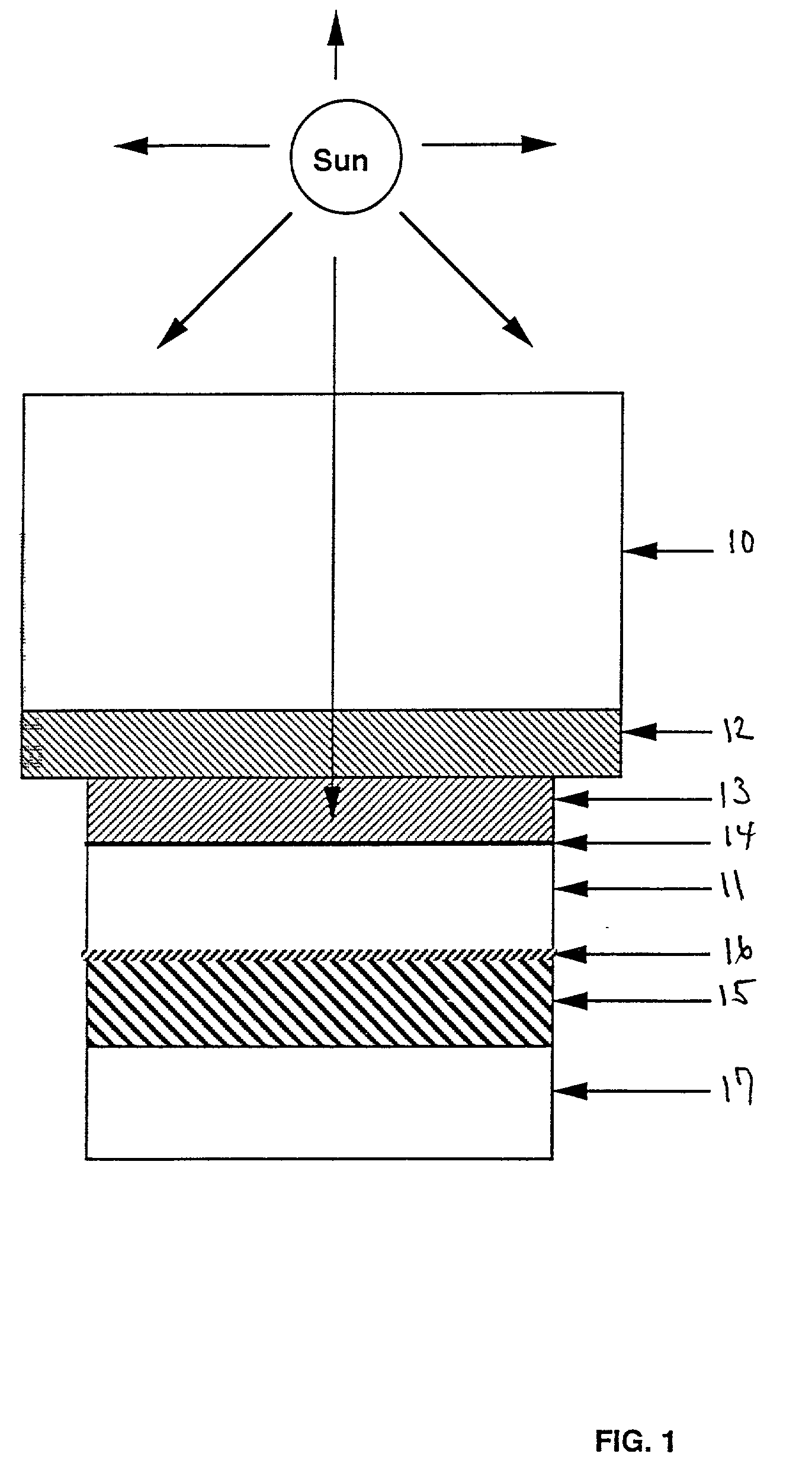
[0040] In this configuration, light enters through the glass substrate 10. The substrate is typically called a superstrate when the cell is designed to have the light incident on the substrate side. The light is absorbed predominantly in the p-CdTe layer 11. The figure shows the location of the transparent-conducting oxide (TCO) layer 12 that forms the transparent electrical top contact to the n-type CdS layer 13, and the location of the semiconductor n-p junction 14 between the n-CdS and p-CdTe. The figure shows the location of a contact-interface layer (CIFL) 15 that optionally may be placed between the CdTe and an outer back metallization to improve the performance of the contact. The interface 16 between the CdTe and the CIFL is where the plasma etching or reactive-ion etching process is applied prior to deposition of the CIFL and / or back metallization or metal back contact 17.EXAMPLE

Problems solved by technology

As an alternative source of electrical energy, photovoltaic technology is under extensive industry research; however, to date, the principal reason why the potential of photovoltaic technology has not been optimally realized is due to the difficulty in preparing photovoltaic devices that efficiently convert light into electricity at costs that are competitive with conventional electrical energy sources.
Nevertheless, the disadvantage associated with single crystalline materials is the high cost of the material as well as the difficulty in depositing the single crystalline materials.
On the other hand, in the case of amorphous materials, one must contend with low carrier mobility, low minority carrier lifetime, low efficiency, and issues of cell stability.
One significant technological problem with CdTe-based devices is that it is difficult to form an ohmic contact to the p-type form of the material.
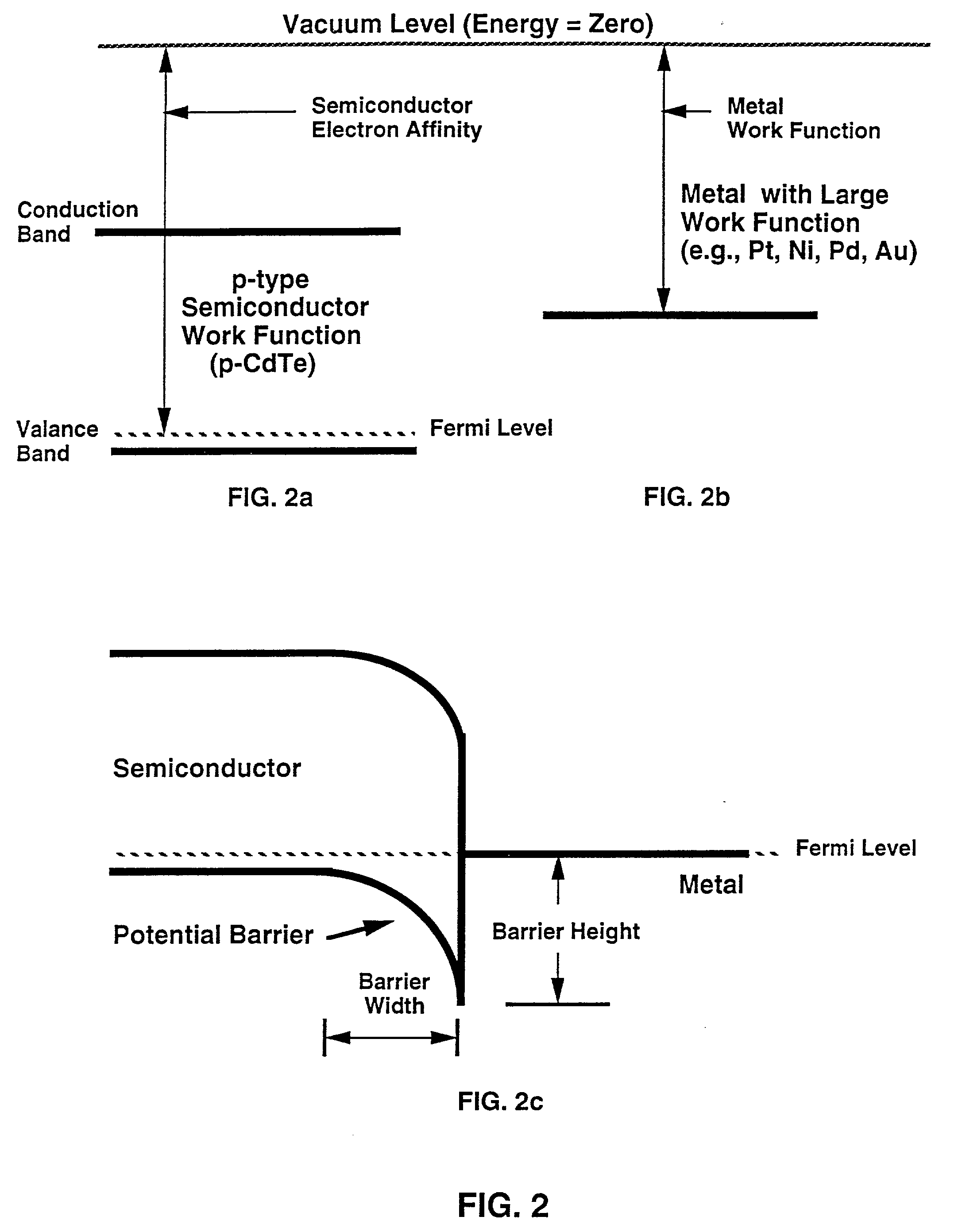
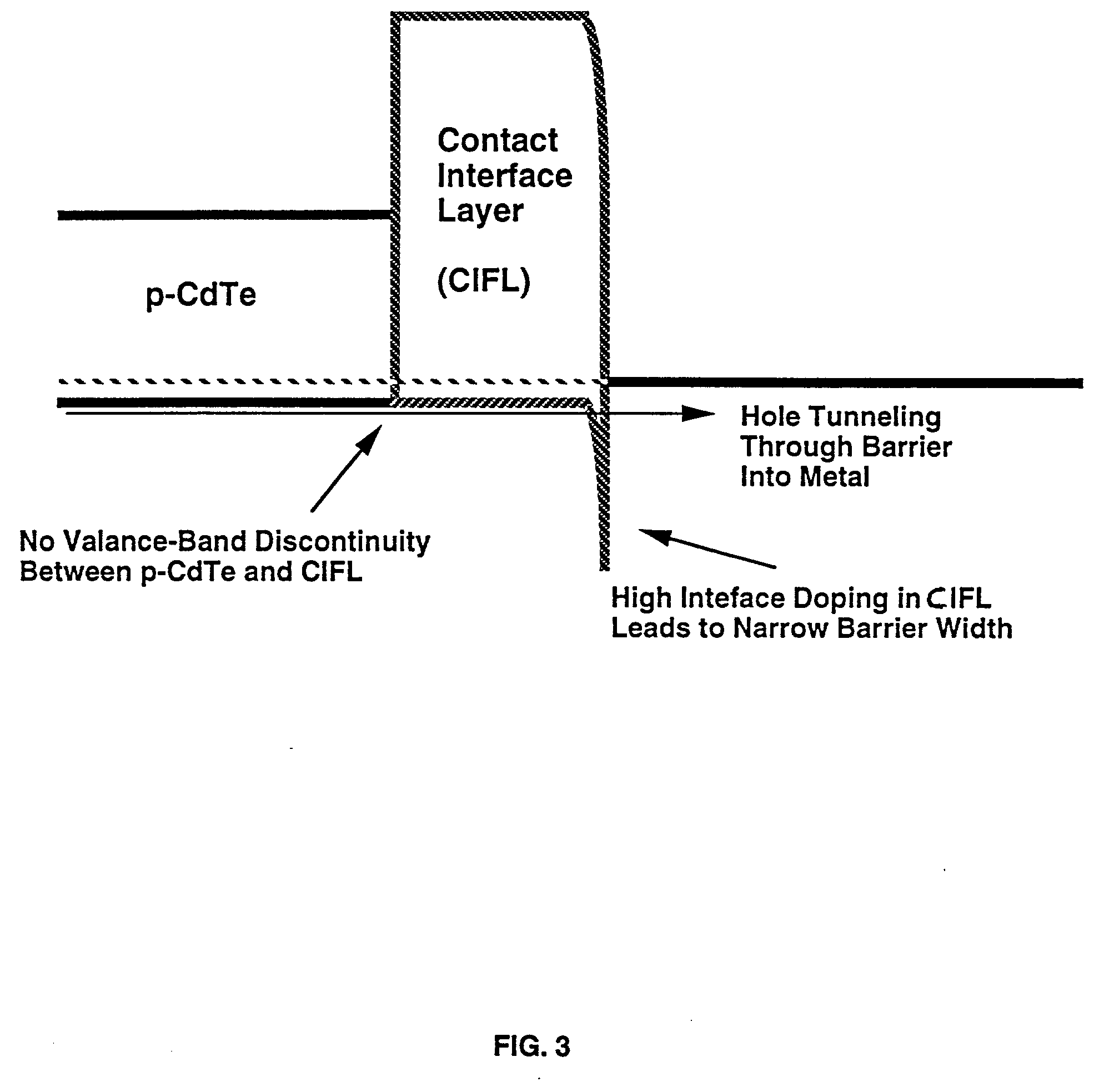
This is observed for both single crystalline and polycrystalline p-type CdTe, and results from a combination of large semiconductor work function, and the inability of CdTe to sustain sufficiently high p-type carrier concentration to enable quantum-mechanical tunneling of charge carriers at the CdTe / metal contact interface.
For the case of p-CdTe and typical metals, the charge carriers will have insufficient energy to flow over the barrier, thus limiting current transport between the metal and semiconductor.
This limitation will lead to contact resistance in solar cell that can become a part of the total series resistance of the solar cell, and thereby limit cell performance.
Note that if a metal with a smaller of work function is chosen, the barrier height will be even larger, further limiting cell performance.
However, because the maximum p-type carrier concentration is limited by compensation mechanisms, low-resistance tunneling has not been demonstrated between metals and p-CdTe.
Although the Te-rich region formed by the wet chemical etching assists the formation of ohmic contact, the extent to which the p-CdTe is effected is dependent on etching parameters, and these are often difficult to control.
gion. It is well known that significant diffusion of certain metals (such as Cu) into the junction region can lead to losses in cell performance and to long-term instab

Method used


Image

  • Plasma & reactive ion etching to prepare ohmic contacts
  • Plasma & reactive ion etching to prepare ohmic contacts
  • Plasma & reactive ion etching to prepare ohmic contacts

Examples


Embodiment Construction

[0041] A CdS / CdTe is placed into a chamber and evacuated to pressures <1e-3 torr using appropriate vacuum pumps. The sample is oriented on a sample holder with the p-CdTe side of the sample facing the plasma region (p-CdTe side up). The sample is positioned on the sample holder to allow for sample heating or cooling. In the case of Reactive Ion Etching (RIE), the sample holder is disposed to provide a radio-frequency (r.f.) bias by an appropriate power supply, capacitive matching network, electrical feedthroughs, and electrical insulation. After the sample is loaded into the processing chamber, the chamber is evacuated to an appropriate base pressure.

[0042] After the base vacuum pressure is established within the processing chamber, the chamber is backfilled with Ar and any other reactive gas species through pressure appropriate for plasma ignition and operation (.about.1e-2 torr). The plasma generates energetic gas species (e.g. electrons, atomic neutrals and ions), and these vario...


PUM

PropertyMeasurementUnit
frequencyaaaaaaaaaa
current efficienciesaaaaaaaaaa

Abstract

A method of making a low-resistance electrical contact between a metal and a layer of p-type CdTe surface by plasma etching and reactive ion etching comprising: a) placing a CdS / CdTe layer into a chamber and evacuating said chamber; b) backfilling the chamber with Argon or a reactive gas to a pressure sufficient for plasma ignition; and c) generating plasma ignition by energizing a cathode which is connected to a power supply to enable the plasma to interact argon ions alone or in the presence of a radio-frequency DC self-bias voltage with the p-CdTe surface.

Description

[0002] This invention relates to processes of using Plasma Etching and Reactive Ion Etching to prepare surfaces of p-CdTe thin films for application of ohmic contacts.[0003] Plasma Etching (PE) and Reactive Ion Etching (RIE) are used to prepare the surface of p-type CdTe films so that wet chemical treatments are avoided. These processes may be used for application in preparing photovoltaic and other devices to improve performance by decreasing the losses associated with the back metal contact.BACKROUND OF THE INVENTION[0004] As an alternative source of electrical energy, photovoltaic technology is under extensive industry research; however, to date, the principal reason why the potential of photovoltaic technology has not been optimally realized is due to the difficulty in preparing photovoltaic devices that efficiently convert light into electricity at costs that are competitive with conventional electrical energy sources. Still, industry is continuing to engage in research in an a...

Claims


Application Information

Patent Timeline
Patent Type & Authority Applications(United States)
IPC IPC(8): C23C14/34H01L21/302H01L21/461H01L21/465H01L31/0224H01L31/073H01L31/18
CPCH01J37/32174H01J2237/3341H01L21/465H01L31/022425H01L31/073H01L31/1828Y02E10/543Y02P70/50
Inventor GESSERT, TIMOTHY A.
Owner ALLIANCE FOR SUSTAINABLE ENERGY
Learn More