Electron-beam excitation laser
a laser and electron beam technology, applied in the field can solve the problems of low light emission efficiency of difficult to cause laser oscillation by current injection, and high oscillation threshold value of conventional electron beam excitation lasers
- Summary
- Abstract
- Description
- Claims
- Application Information
AI Technical Summary
Problems solved by technology
Method used
Image
Examples
embodiment 1
[0078] Specifically, Nb film 100 nm thick was formed on a quartz substrate, then aluminum film 1 .mu.m thick was formed on the Nb film by DC sputtering. Next, as is the case with Embodiment 1, the aluminum film was anodized to make alumina nanoholes. These nanoholes were formed at 140 nm intervals in honeycomb formation. Then the aluminum film was anodized at 56 V, using a 0.3M phosphoric acid bath. Finally, the film was subjected to pore wide treatment, that is, immersed in a 5 wt % phosphoric acid solution at 25.degree. C. for 50 minutes to enlarge nanoholes until their diameter reached about 110 nm.
[0079] By electrodeposition, the nanoholes were filled with ZnO to make a light emitter. The substrate was immersed in a 0.1M zinc nitrate solution at 60.degree. C. together with an opposite Pt electrode. Next, a voltage of about -5 V was applied to the substrate to form ZnO crystals In the nanoholes. In Embodiment 7, ZnO crystals were let to grow until they protruded from the nanohole...
embodiment 11
[0084] In Embodiment 11, a laser structure which uses a GRINSH (graded index separate confinement) type ZnCdSe / ZnSe heterostructure produced by MBE for a light emitter was made and evaluated. The laser structure corresponds to FIG. 12A. The light emitter has a heterostructure. The heterostructure consists of a 1 .mu.m thick ZnSe buffer layer on an InGaAs (100) substrate and a quantum well which is made from Zn.sub.0.75Cd.sub.0.25Se interposed between refractive-index change layers of Zn1-xCdxSe (x=0 to 0.05) and is disposed on top of the buffer layer. The refractive-index change layer is 500 nm thick.
embodiment 2
[0085] A reflector made from anodized alumina was formed on the heterostructure in the same was to make the laser structure. In the embodiment, start points were arrayed at 170-nm intervals in honeycomb formation, and anodization was performed at 68 V in a 0.3M phosphoric acid bath. Finally, the laser structure was subjected to pore wide treatment, that is, immersed in a 5 wt % phosphoric acid solution at 25.degree. C. for 70 minutes to enlarge nanoholes until their diameter reached about 140 nm.
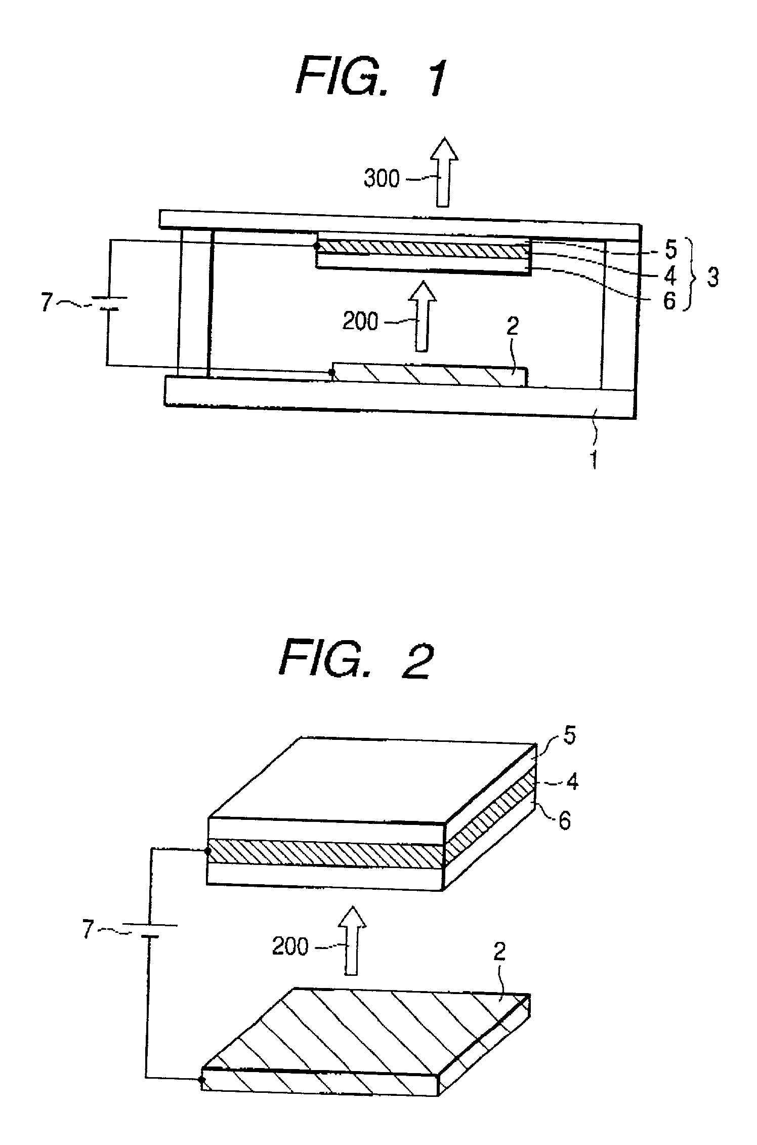
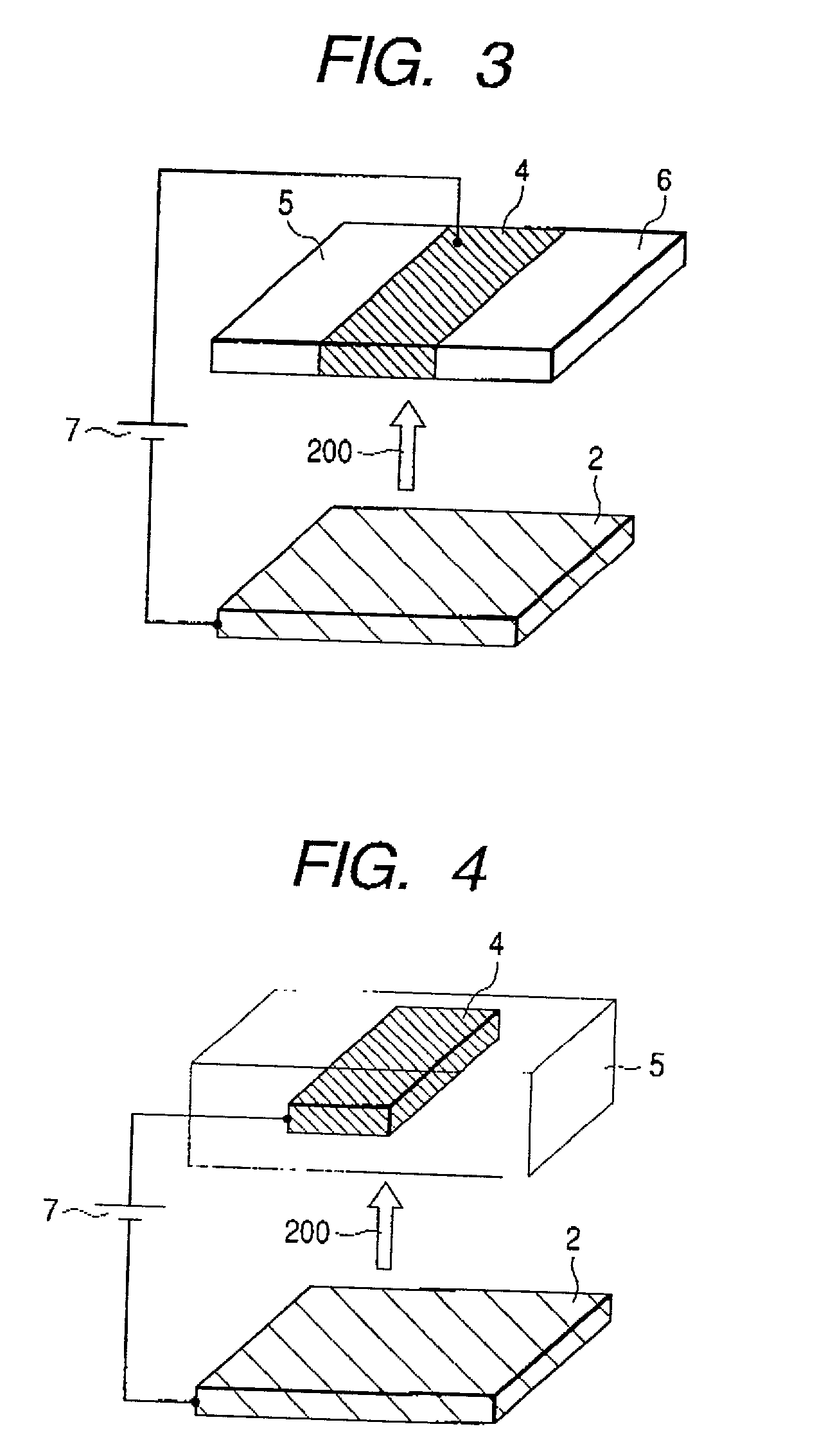
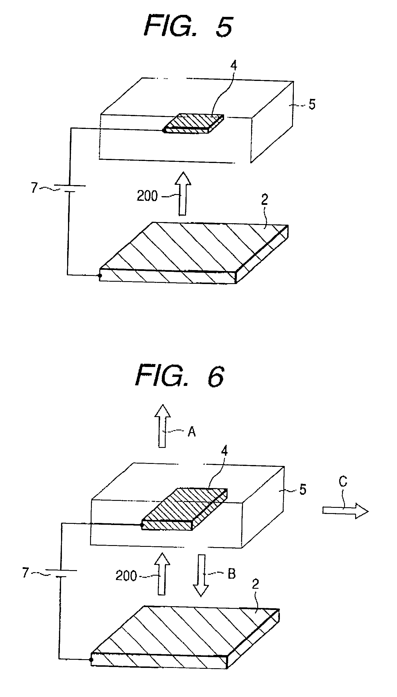
[0086] A spint type electron source was provided which has 10.sup.4 to 10.sup.5 Mo chips per square millimeter. The thus produced laser structure was placed opposite to the spint type electron source in a glass container. After the container was evacuated, it was hermetically sealed. As electron accelerating means, a high-voltage power supply was connected to the electron source and laser structure. When a beam of electrons accelerated to an acceleration voltage of 10 to 50 keV was irradiat...
PUM
 Abstract
Description
Claims
Application Information
 - R&D
- Intellectual Property
- Life Sciences
- Materials
- Tech Scout
- Unparalleled Data Quality
- Higher Quality Content
- 60% Fewer Hallucinations
Browse by: Latest US Patents, China's latest patents, Technical Efficacy Thesaurus, Application Domain, Technology Topic, Popular Technical Reports.
© 2025 PatSnap. All rights reserved.Legal|Privacy policy|Modern Slavery Act Transparency Statement|Sitemap|About US| Contact US: help@patsnap.com


