Diamond wafer, method of estimating a diamond wafer and diamond surface acoustic wave device

a diamond wafer and surface acoustic wave technology, applied in the direction of crystal growth process, transportation and packaging, natural mineral layered products, etc., can solve the problems of large propagation loss in diamond saw devices, sapphire saw devices, quartz saw devices or linbo.sub.3 saw devices still unsatisfactory for high frequency filters, and diamond saw devices still unpractical

Inactive Publication Date: 2001-11-22
SUMITOMO ELECTRIC IND LTD
View PDF0 Cites 9 Cited by
  • Summary
  • Abstract
  • Description
  • Claims
  • Application Information

AI Technical Summary

Benefits of technology

[0013] The insulator which has been most widely used as the material of the rigid base is glass. Glass is an inexpensive and low-loss insulator. ZnO / glass SAW filters have been popularly employed as TV intermediate frequency filters. Zinc oxide (ZnO) is a piezoelectric material. ZnO / glass means a SAW filter having a glass substrate and a ZnO film deposited on the glass. In spite of low-loss and low-cost, glass SAW devices cannot raise operation frequency f.sub.0 owing to the low SAW velocity v. Somebody has proposed new SAW devices having a harder rigid base than glass, for example, sapphire, quartz, LiNbO.sub.3 and so on. These new materials give higher SAW velocity than glass owing to high Young's modulus. However, the SAW velocities of sapphire SAW devices, quartz SAW devices or LiNbO.sub.3 SAW devices are still unsatisfactory for high frequency filters. Diamond is the most promising candidate which gives the highest SAW velocity due to the extreme rigidity.
[0015] Since the frequency f is very high, the wavelength .lambda.=v / f is reduced to a similar size to the micro-cavities and micro-convexities. Acoustic phonons building the surface acoustics wave are scattered by the micro-defects, because phonons are mostly perturbed by the objects of the same size as the wavelength. Besides the high propagation loss .DELTA.Ep, the defects-rich diamond film decreases the yield of SAW devices by raising the rate of electrode-pattern cutting. Micro-defects prevent diamond SAW devices from growing to practical SAW devices through the large propagation loss .DELTA.Ep and the low yield. Here "yield" means a ratio of the number of good products to the number of all products.
[0016] One purpose of the present invention is to produce diamond SAW devices having low propagation loss. Another purpose of the present invention is to enhance the yield of the diamond SAW devices. In addition to SAW devices, this invention can be applied to raising the yield of the production of microelectronic devices or micromachines making use of small wire patterns with a breadth less than 5.0 .mu.m through reducing the rate of the wiring pattern cutting.
[0017] Higher frequency requires SAW filters to make a still better piezoelectric film. The undercoating diamond film must be flat, smooth and defect-free for producing (Diamond) / (piezoelectric material) SAW devices. For this purpose, a simple and reliable estimation technique of diamond films is indispensable besides fabrication of good diamond films. This invention proposes also a method for easily estimating diamond films.

Problems solved by technology

However, the SAW velocities of sapphire SAW devices, quartz SAW devices or LiNbO.sub.3 SAW devices are still unsatisfactory for high frequency filters.
Diamond SAW devices enable the current lithography technology to pattern interdigital transducers for a frequency higher than 1 GHz owing to the high SAW velocity v. However, the propagation loss .DELTA.Ep is still large in diamond SAW devices.
The large propagation loss .DELTA.Ep leaves diamond SAW devices impractical.
It is difficult to make a wide, flat, even, smooth and defect-free diamond film covering the whole of the device due to the extreme rigidity of diamond.
It is further difficult to make a flat piezoelectric film on the defect-rich diamond film.
Even if the piezoelectric film is produced, it is still a piezoelectric film of poor quality.
Many defects on the diamond surface and the shortness of the SAW wavelength raise the propagation loss .DELTA.Ep and leave diamond SAW devices inoperative.
Besides the high propagation loss .DELTA.Ep, the defects-rich diamond film decreases the yield of SAW devices by raising the rate of electrode-pattern cutting.
Micro-defects prevent diamond SAW devices from growing to practical SAW devices through the large propagation loss .DELTA.Ep and the low yield.
However, the field of vision is too narrow.
It would take very much time to observe the whole surface of a SAW device by microscopes.
Microscope observation cannot be applied to the examination of diamond surfaces in the process of producing diamond SAW devices.
Namely, there is no estimation method available for examining diamond surface on an industrial scale.
A laser scanning surface defect detection apparatus for silicon wafers cannot be readily used for estimating a diamond.
However, the photomultiplier can also detect geometrical surface defects. FIG. 14 shows a notch, a surface defect, on the surface of the silicon wafer.
It takes only a short time to examine a pretty wide silicon wafer by the laser scanning surface defect detection apparatus.
However, the laser scanning surface defect detection apparatus cannot be readily used to examine the surface of diamond.
For this reason, the laser scanning surface defect detection apparatus cannot be applied to the examination of the surface of diamond.
If the diamond has defects or dust, the coating layer has similar anomalies due to the defects or dust at the same spots.
However, defect detection is a problem.
If a wafer has a big inner stress, the mother materials, silicon or a metal, will be distorted.
Although many proposals have been discussed and proved that diamond SAW devices would be superior in the SAW velocity to other materials, diamond SAW devices are suffering from extremely low yield due to the large propagation loss of the SAW devices having piezoelectric films upon diamonds.
The low yield resulted from the lack of the method of a preliminary examination of diamond crystals.
Since the property of diamond films could not be measured, SAW devices made on the property-unknown diamond crystals were tested, which lowered the yield and raised the production cost.
The laser scanning surface defect detection apparatus cannot be employed for examining diamond surfaces as it is.
However, the ultrahigh pressure method can make only a small-sized diamond crystal.

Method used


Image

  • Diamond wafer, method of estimating a diamond wafer and diamond surface acoustic wave device
  • Diamond wafer, method of estimating a diamond wafer and diamond surface acoustic wave device
  • Diamond wafer, method of estimating a diamond wafer and diamond surface acoustic wave device

Examples


embodiment 2

of Propagation Loss on Samples Having Piezoelectric Films

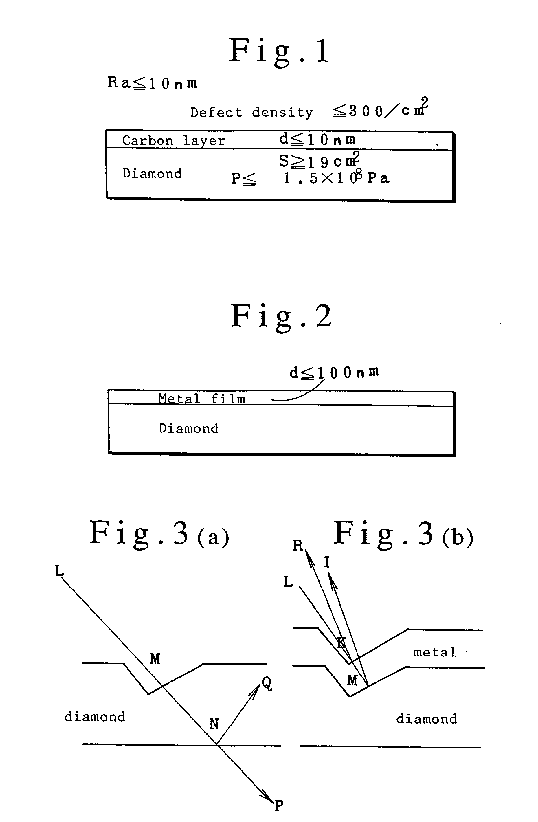
[0092] The previous test tells us that sample A and sample B of less than 300 defects / cm.sup.2 are immune from electrode breaking. However the defect estimation is not sufficient to know the performance of SAW devices which are going to be made by depositing piezoelectric films and electrodes on the diamond substrates. Then, actual propagation loss was measured on SAW devices made by depositing piezoelectric films on the dia / Si wafers of sample A and sample B which passed the defect test and forming interdigital transducers on the piezoelectric films. No SAW devices were made on samples C to J which failed in the defect test.

[0093] 1. Formation of Piezoelectric Films

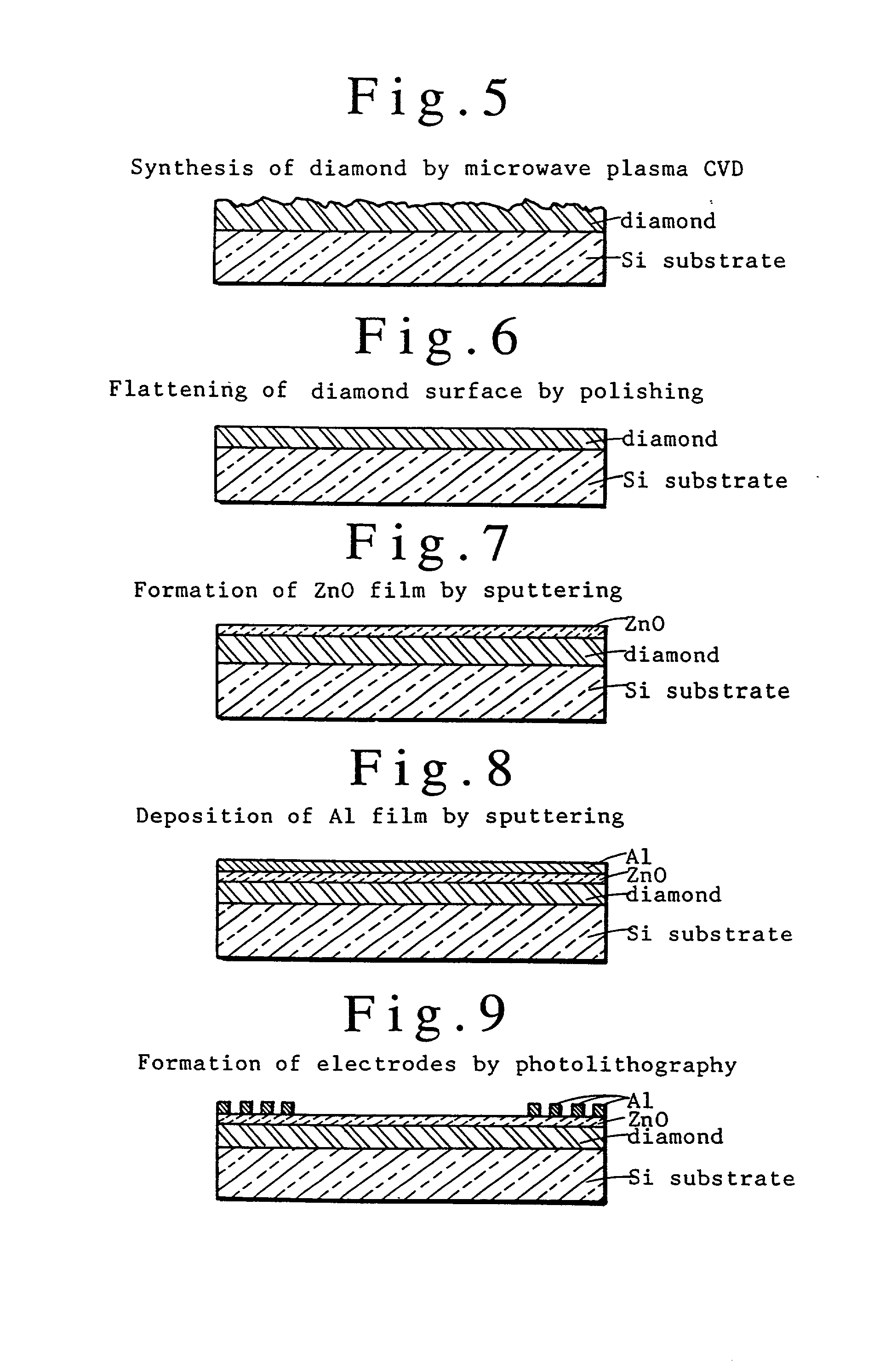
[0094] Piezoelectric ZnO films of a 1050 nm thickness were formed upon the dia / Si substrates of sample A and sample B by an RF sputtering method.

[0095] (Condition of Formation of ZnO Piezoelectric Film)

4 Substrates dia / Si wafers: sample A, sample B Target ZnO sinte...


PUM

PropertyMeasurementUnit
heightsaaaaaaaaaa
areaaaaaaaaaaa
thicknessaaaaaaaaaa

Abstract

Surfaces of diamond crystals are examined by coating the surfaces with thin metal films, launching laser beams to the diamond surfaces in a slanting angle, detecting defects and particles on the diamond surfaces by the scattering of beams and counting the defects and particles by a laser scanning surface defect detection apparatus. Diamond SAW devices should be made on the diamond films or bulks with the defect density less than 300 particles cm-2. Preferably, the diamond surfaces should have roughness less than Ra20 nm. Diamond SAW filters can be produced by depositing a piezoelectric film and making interdigital transducers on the low-defect density diamond crystals.

Description

[0001] 1. Field of the Invention[0002] This invention relates generally to a diamond wafer and a surface acoustic wave (SAW) device produced on the diamond wafer. This invention relates more specially to a method of estimating diamond wafers which judges whether a diamond wafer is suitable for producing SAW devices or not. The estimation selects diamond wafers that have a low density of surface defects which enables manufacturers to produce a low loss SAW device. The diamond wafers can also be used as the substrates of microelectronic devices with microscopic wiring or the substrates of micromachines with microscopic structures.[0003] This application claims the priority of Japanese Patent Application No.9-290262 (290262 / 97) filed Oct. 6, 1997 which is incorporated herein by reference.[0004] 2. Description of Related Art[0005] Diamond enjoys the highest sound velocity among all the natural materials. The hardness is also the highest. The thermal conductivity is large. The band gap o...

Claims


Application Information

Patent Timeline
Patent Type & Authority Applications(United States)
IPC IPC(8): C30B29/04C23C14/34G01N21/47G01N21/88H01L41/09H03H3/08H03H9/02H03H9/25
CPCH03H3/08H03H9/02582Y10T428/24975Y10T428/265Y10T428/24917Y10T428/30Y10T428/24479Y10T428/31678
Inventor FUJII, SATOSHISEKI, YUICHIROYOSHIDA, KENTARONAKAHATA, HIDEAKIHIGAKI, KENJIROKITABAYASHI, HIROYUKIUEMURA, TOMOKISHIKATA, SHIN-ICHI
Owner SUMITOMO ELECTRIC IND LTD
Why Eureka
Try Eureka