Method of manufacturing a semiconductor device

a manufacturing method and semiconductor technology, applied in semiconductor devices, instruments, optics, etc., can solve the problems of inability to control the crystal orientation, limitations in the properties of tft, and the possibility of increasing the crystal orientation arrangement to become more unidirectional

Inactive Publication Date: 2002-10-17
SEMICON ENERGY LAB CO LTD
View PDF82 Cites 55 Cited by
  • Summary
  • Abstract
  • Description
  • Claims
  • Application Information

AI Technical Summary

Benefits of technology

[0013] One element, or a plurality of elements, selected from the group consisting of H, H.sub.2, O, O.sub.2 and P may also be added in addition to the inert gas element. A synergistic gettering effect can be obtained by thus adding a plurality of elements. Among the group, O and O.sub.2 are particularly effective, and gettering efficiency is increased if oxygen concentration added during or after film formation is equal to or greater than 5.times.10.sup.18 / cm.sup.3 within the second semiconductor film and the third semiconductor film as measured by SIMS analysis, preferably in a concentration range from 1.times.10.sup.19 / cm.sup.3 to 1.times.10.sup.22 / cm.sup.3. Note that inert gas elements have almost no diffusion. If another element added in addition to the inert gas element diffuses easily, then it is preferable to regulate the film thickness of the second semiconductor film such that the other added element does not diffuse to the first semiconductor film due to later heat treatment processes. Furthermore, in addition to the second semiconductor film, the barrier layer also functions to prevent diffusion of the other element.

Problems solved by technology

It is impossible to control the crystal orientation, and this consequently causes limitations in properties of the TFT.
This not only has an effect of lowering a heating temperature required for crystallization, but it also becomes possible to increase the crystal orientation arrangement to become more unidirectional.
However, if a metallic element having a catalytic action for crystallization is added, the metallic element remains within the crystalline semiconductor film or on the surface of the film, and there are problems such as fluctuation in properties of elements obtained.
Examples thereof include problems such as an increase in an off current in the TFT and its fluctuation between the individual elements.
That is, the metallic elements that have a catalytic action for crystallization exist unnecessarily after the crystalline semiconductor film is formed.
Adding phosphorous by ion doping can cause a crystalline semiconductor film to take on amorphous qualities, and the increase in the phosphorous concentration hinders recrystallization during a later annealing process, thus becoming a problem.
Further, the addition of a high concentration of phosphorous causes an increase in the required amount of processing time for doping, and throughput of the doping process step is decreased, thus becoming a problem.

Method used


Image

  • Method of manufacturing a semiconductor device
  • Method of manufacturing a semiconductor device
  • Method of manufacturing a semiconductor device

Examples


embodiment

[0090] Embodiment mode 2

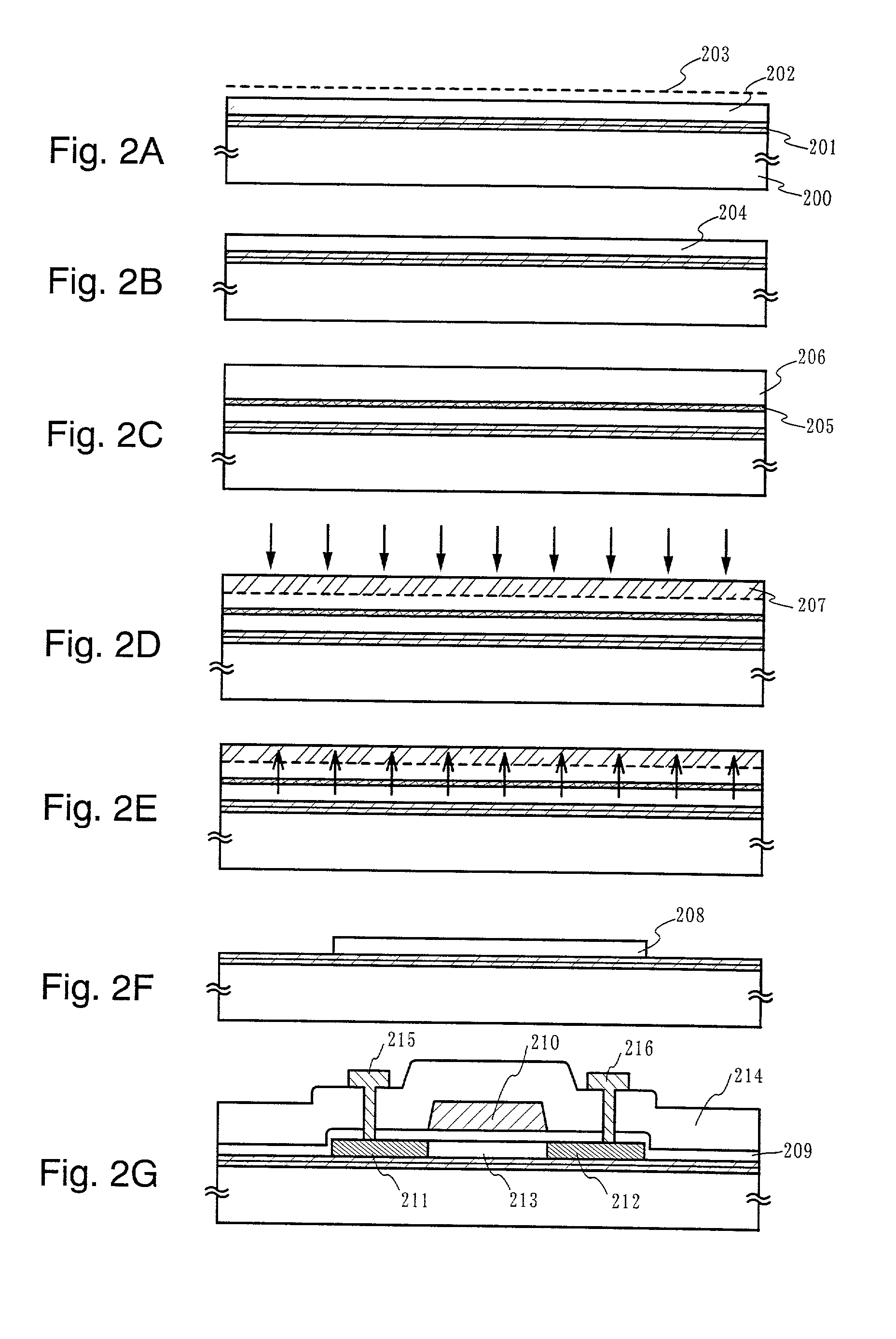
[0091] Gettering sites may also be formed by adding an inert gas element to only the upper layer of the second semiconductor film, without forming the third semiconductor film, shown in Embodiment mode 1. An example of this is explained here using FIGS. 2A to 2G.

[0092] Manufacturing up through the formation of a barrier layer 205 is similar to that of Embodiment mode 1. A base insulating film 201 is formed on a substrate 200, and the barrier layer 205 is formed after forming a semiconductor film 204 having a crystalline structure, all in accordance with Embodiment mode 1. Crystallization is also performed here using nickel, as in Embodiment mode 1. Note that FIG. 2A corresponds to FIG. 1A, and that FIG. 2B corresponds to FIG. 1B.

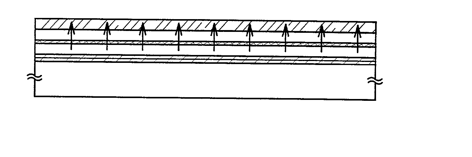
[0093] A second semiconductor film 206 is formed next on the barrier layer 205. (See FIG. 2C.) The second semiconductor film 206 contains an inert gas element. A semiconductor film having an amorphous structure may be formed, and a se...

embodiments

[0100] Embodiment 1

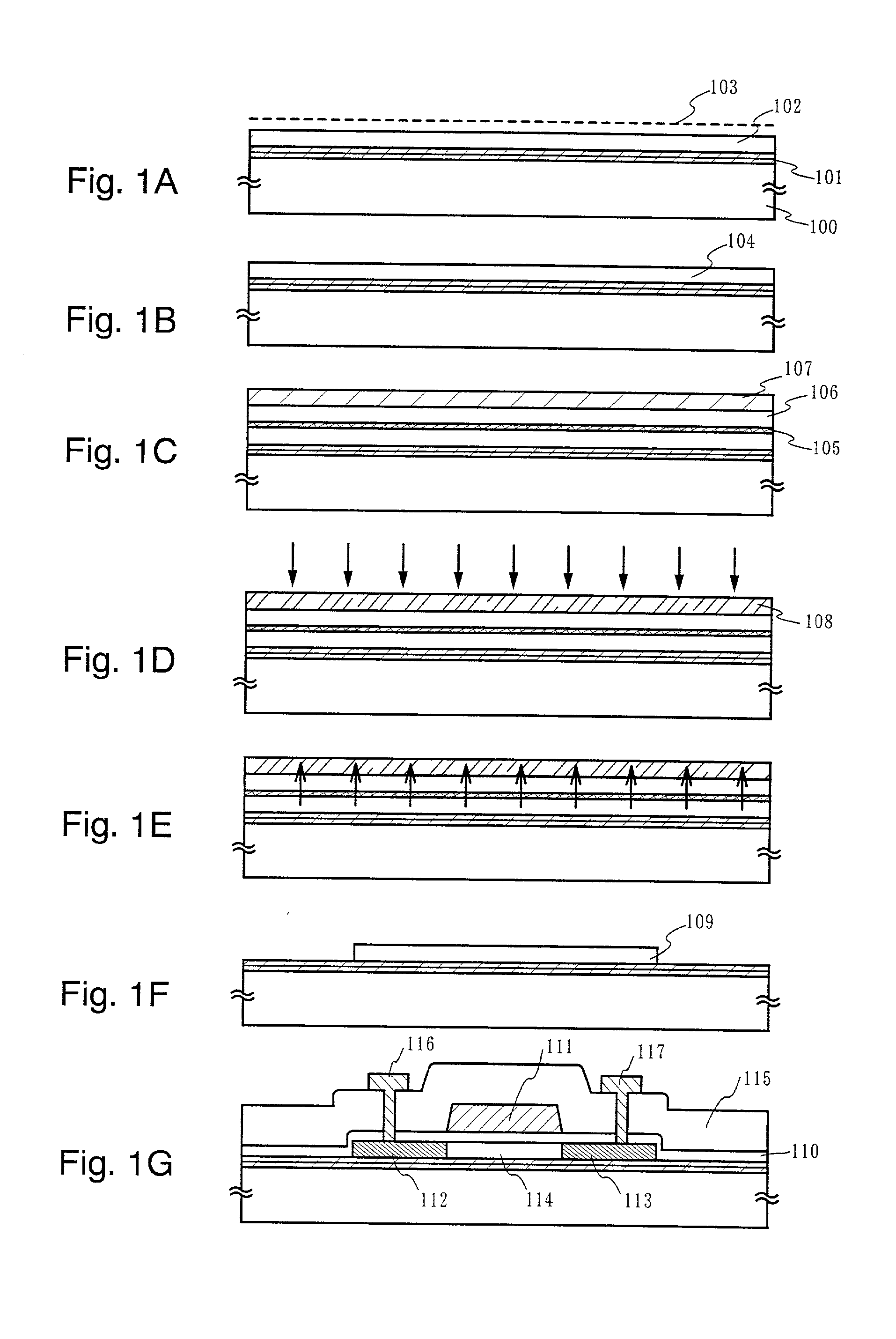
[0101] Here, a method of manufacturing a pixel portion and driver circuit TFTs (an n-channel TFT and a p-channel TFT) formed in the periphery of the pixel portion at the same time and on the same substrate is explained using FIGS. 3A to 5.

[0102] First, a substrate 300 made from a glass such as barium borosilicate glass or aluminum borosilicate glass, typically Coming Corp. #7059 glass or #1737 glass, is used in Embodiment 1. Note that, provided that the substrate has transparency to light, a quartz substrate may also be used as the substrate 300. Further, a plastic substrate having resistance to heat that is able to withstand the processing temperatures of Embodiment 1 may also be used.

[0103] Next, a base film 301 made from an insulating film such as a silicon oxide film, a silicon nitride film, or a silicon oxynitride film is formed on the substrate 300. A two layer structure is used as the base film 301 in Embodiment 1, but a single layer insulating film or one ...

embodiment 2

[0135] Embodiment 2

[0136] An example of performing crystallization by a method which differs from that of Embodiment mode 1 is shown in FIGS. 6A to 6D in Embodiment 2.

[0137] First, a base insulating film 701 and an amorphous semiconductor film 702 are formed on a substrate 700, as in Embodiment mode 1. An insulating film having silicon as its main constituent is formed next, and a mask 703 made from resist is formed. The insulating film is then selectively removed using the mask 703, forming a mask 704. (See FIG. 6A.)

[0138] A metallic element containing layer 705 is then formed after removing the mask 703. The metallic element is selectively added to the amorphous semiconductor film positioned in regions not covered with the mask 704 here. (See FIG. 6B.)

[0139] A heat treatment process is performed next, causing crystallization, and a semiconductor film 706 having a crystalline structure is formed. The heat treatment process using an electric furnace or the irradiation of strong ligh...


PUM

PropertyMeasurementUnit
temperatureaaaaaaaaaa
thicknessaaaaaaaaaa

Abstract

An object is to reduce the number of high temperature (equal to or greater than 600° C.) heat treatment process steps and achieve lower temperature (equal to or less than 600° C.) processes, and to simplify the process steps and increase throughput in a method of manufacturing a semiconductor device. With the present invention, a barrier layer, a second semiconductor film, and a third semiconductor film containing an inert gas element are formed on a first semiconductor film having a crystalline structure. Gettering is performed and a metallic element contained in the first semiconductor film passes through the barrier layer and the second semiconductor film by a heat treatment process, and moves to the third semiconductor film. The second semiconductor film and the third semiconductor film are then removed, with the barrier layer used as an etching stopper.

Description

[0001] 1. Field of the Invention[0002] The present invention relates to a method of manufacturing a semiconductor device using a gettering technique. In particular, the present invention relates to a method of manufacturing a semiconductor device that uses a crystalline semiconductor film manufactured by adding a metallic element having a catalytic action in crystallizing a semiconductor film.[0003] Note that, throughout this specification, the term semiconductor device indicates general devices capable of functioning by utilizing semiconductor properties. Electro-optical devices, semiconductor circuits, and electronic devices are all semiconductor devices.[0004] 2. Description of the Related Art[0005] Thin film transistors (hereafter referred to as TFTs) are known as typical semiconductor elements that use a semiconductor film having a crystalline structure (hereafter referred to as crystalline semiconductor film). TFTs are in the spotlight as a technique of forming an integrated c...

Claims


Application Information

Patent Timeline
Patent Type & Authority Applications(United States)
IPC IPC(8): G02F1/1368G02F1/1362H01L21/322H01L21/336H01L21/768H01L21/77H01L21/84H01L27/12H01L29/786
CPCG02F1/13454H01L27/12H01L29/66757H01L27/1277H01L29/78624H01L29/78675H01L29/78678H01L29/78621
Inventor YAMAZAKI, SHUNPEINAKAMURA, OSAMUKAJIWARA, MASAYUKIKOEZUKA, JUNICHIDAIRIKI, KOJIMITSUKI, TORUTAKAYAMA, TORUOHNUMA, HIDETOASAMI, TAKETOMIICHIJO, MITSUHIRO
Owner SEMICON ENERGY LAB CO LTD
Why Eureka
Try Eureka