Masking methods and etching sequences for patterning electrodes of high density RAM capacitors

a patterning electrode technology, applied in the field of masking methods and etching sequences for patterning electrodes of high density ram capacitors, can solve the problems of deteriorating processing accuracy, insufficient fine pattern processing precision of isotropic etching, and difficulty in performing submicron patterning of platinum electrodes

Inactive Publication Date: 2003-03-27
APPLIED MATERIALS INC
View PDF0 Cites 47 Cited by
  • Summary
  • Abstract
  • Description
  • Claims
  • Application Information

AI Technical Summary

Problems solved by technology

Because of the nature of isotropic etching, using wet etching with aqua regia causes deteriorated processing accuracy.
The grade of precision in isotropic etching is not high enough for fine pattern processing.
Therefore, it is difficult to perform submicron patterning of platinum electrodes due to its isotropic property.
Furthermore, a problem with ion milling (i.e., anisotropic etching) occurs because the etching speed on platinum and iridium, which is to form the electrode, is too slow for mass production.
Yoo et al. found that a major problem of etching with a MERlE was the redeposition of the etch products onto the pattern sidewall, making it difficult to reduce the pattern size.
To eliminate the problem of fencing, it is possible to etch the fence layer and erode the sides of the photoresist during the etch process which leads to "clean" metal structures but with sloping sidewall angles and a loss of control over critical feature sizes.
The existence of such structures makes useful deposition of the PZT layer impossible.
Although process conditions can be found which result in either low redeposition or even no redeposition, they most often also give an unacceptably tapered platinum profile angle.
While a post etch wet clean in a solvent bath is frequently used, the heavy redeposition which attends the pursuit of vertical sidewalls regularly renders this approach minimally effective.
Where as vigorous post etch cleaning (e.g., wet cleaning with acid, mechanical polishing, etc.) can relieve some of the need to achieve a deposition free plasma etch, such post etch cleaning does not possess the accuracy that is desired as the platinum electrode itself is typically eroded and / or deteriorated by currently known post etch cleaning methods.
The patterned resist layer is removed from the residual mask layer before heating the substrate to a temperature greater than about 150.degree. C. because such high temperatures would destroy the resist layer.

Method used


Image

  • Masking methods and etching sequences for patterning electrodes of high density RAM capacitors
  • Masking methods and etching sequences for patterning electrodes of high density RAM capacitors
  • Masking methods and etching sequences for patterning electrodes of high density RAM capacitors

Examples


example i

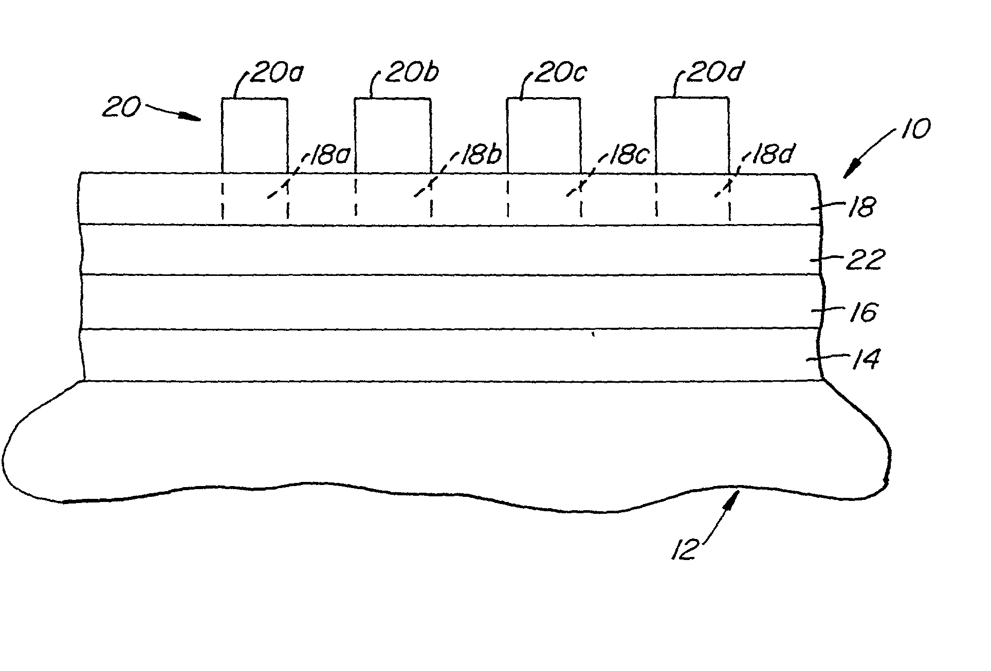
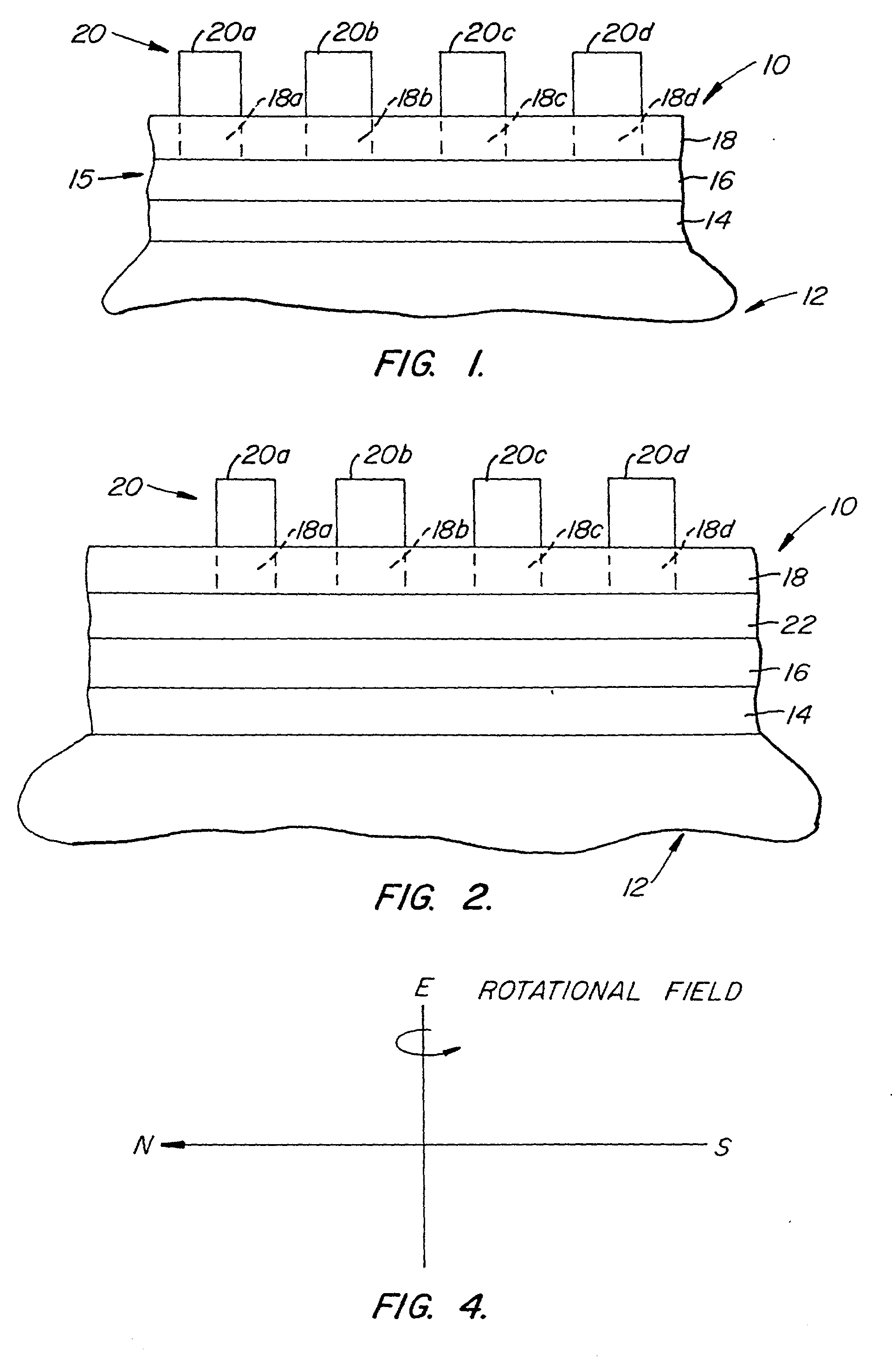
[0256] A test semiconductor wafer was formulated with the following film stack:

0.8 .mu.m patterned PR (photoresist) / 5000 .ANG. Oxide / 1000 .ANG. Ti / 1000 .ANG. Pt / 300 .ANG. TiN

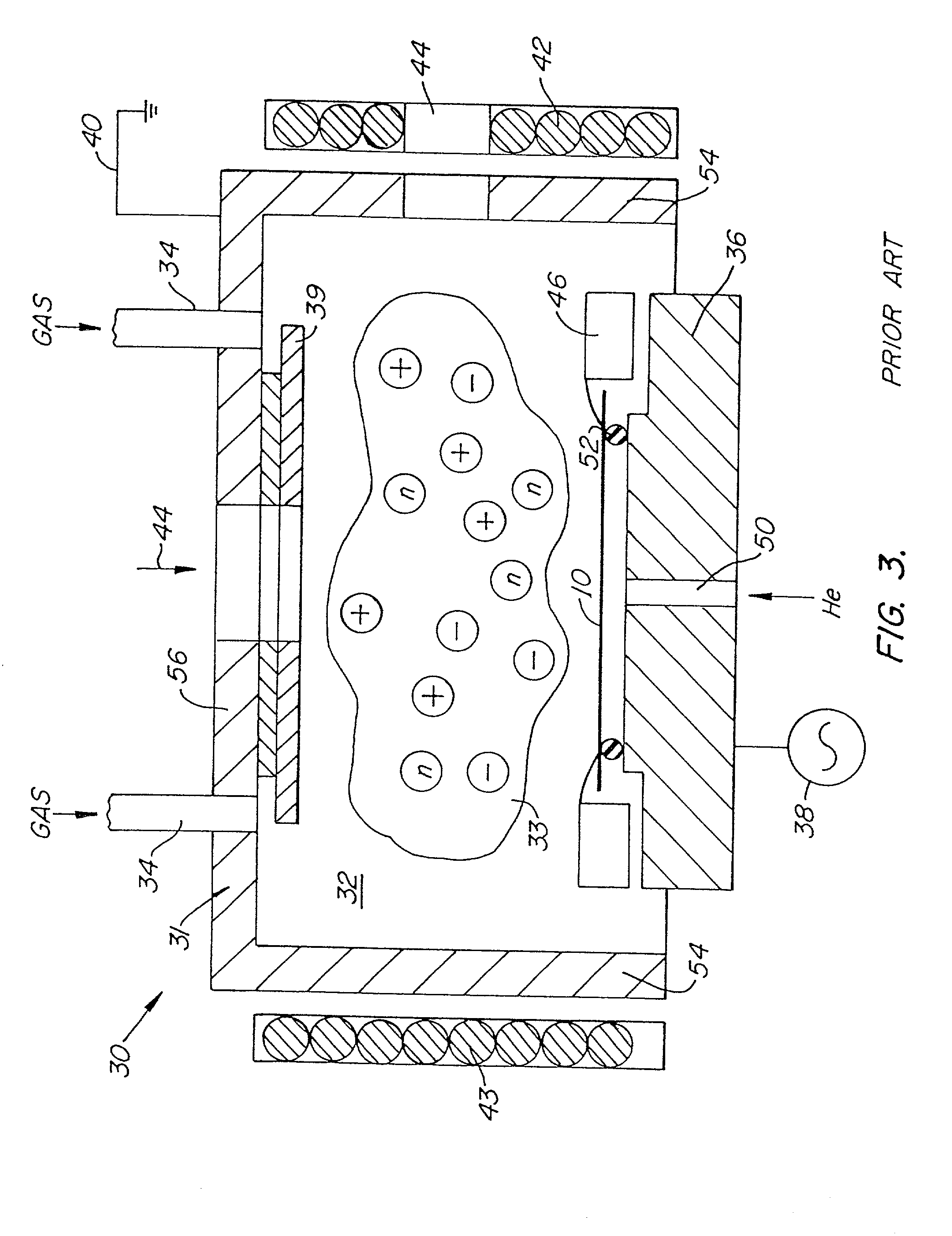
[0257] The feature size of the patterned PR test semiconductor wafer was 0.3 .mu.m block and 0.25 .mu.m spacing. The oxide mask (i.e., the mask layer) was opened in the oxide etch chamber of a plasma processing apparatus sold under the trademark Oxide Etch MxP Centura.TM., owned by Applied Materials Inc., 3050 Bowers Avenue, Santa Clara, Calif. 95054-3299. The etchant gas for opening the oxide mask comprised about 68% by volume Ar and about 32% by volume CHF.sub.3. The reactor and process conditions were as follows:

37 Reactor Conditions Pressure 60 mTorr RF Power 850 watts Rotational Magnetic Field 40 Gauss Temperature of Test Wafer 100.degree. C. Oxide Mask Etch Rate 3000 .ANG. / min Process Conditions Based on the Flow Rate of Ar and CHF3 CHF.sub.3 50 sccm Ar 100 sccm Pressure, mTorr 60 mTorr RF Power Density 85...

example ii

[0263] A test semiconductor wafer was formulated with the following film stack:

0.8 .mu.m patterned PR (photoresist) / 5000 .ANG. Oxide / 600 .ANG. TiN / 2000 .ANG. Pt / 300 .ANG. TiN

[0264] The feature size of the patterned PR test semiconductor wafer was 0.25 .mu.m block and 0.2 .mu.m spacing. The oxide mask (i.e., the mask layer) was opened in the oxide etch chamber of a plasma processing apparatus sold under the trademark Oxide Etch MxP Centura.TM., owned by Applied Materials Inc., 3050 Bowers Avenue, Santa Clara, Calif. 95054-3299. The etchant gas for opening the oxide mask comprised about 68% by volume Ar and about 32% by volume CHF.sub.3. The reactor and process conditions were as follows:

41 Reactor Conditions Pressure 60 mTorr RF Power 850 watts Rotational Magnetic Field 40 Gauss Temperature of Test Wafer 100.degree. C. Oxide Mask Etch Rate 3000 .ANG. / min

[0265]

42 Process Conditions Based on the Flow Rate of Ar and CHF.sub.3 CHF.sub.3 50 sccm Ar 100 sccm Pressure, mTorr 60 mTorr RF Pow...

example iii

[0272] A test semiconductor wafer was formulated with the following film stack:

1.2 .mu.m patterned PR (photoresist) / 5000 .ANG. TEOS / 200 .ANG. TiN / 2500 .ANG. Pt / 300 .ANG. TiN / 500 .ANG. SiN.

[0273] The feature size of the patterned PR test semiconductor wafer was 0.35 .mu.m line and 0.35 .mu.m spacing. The TEOS mask (i.e., the mask layer) was opened in the oxide etch chamber of a plasma processing apparatus sold under the trademark Oxide Etch MxP Centura.TM., owned by Applied Materials Inc., 3050 Bowers Avenue, Santa Clara, Calif. 95054-3299. The etchant gas for opening the TEOS mask comprised about 68% by volume Ar and about 32% by volume CHF.sub.3. The reactor and process conditions were as follows:

47 Reactor Conditions Pressure 60 mTorr RF Power 850 watts Rotational Magnetic Field 40 Gauss Temperature of Test Wafer 100.degree. C. TEOS Mask Etch Rate 3000 .ANG. / min Process Conditions Based on the Flow Rate of Ar and CHF.sub.3 CHF.sub.3 50 sccm Ar 100 sccm Pressure, mTorr 60 mTorr RF ...


PUM

PropertyMeasurementUnit
temperatureaaaaaaaaaa
dielectric constantaaaaaaaaaa
thicknessaaaaaaaaaa

Abstract

A method of etching a noble metal electrode layer disposed on a substrate to produce a semiconductor device including a plurality of electrodes separated by a distance equal to or less than about 0.35 mum and having a noble metal profile equal to or greater than about 80°. The method comprises heating the substrate to a temperature greater than about 150° C., and etching the noble metal electrode layer by employing a high density inductively coupled plasma of an etchants gas comprising a gas selected from the group consisting nitrogen, oxygen, a halogen (e.g., chlorine), argon, and a gas selected from the group consisting of BCl3, HBr, and SiCl4 mixtures thereof. A semiconductor device having a substrate and a plurality of noble metal electrodes supported by the substrate. The noble metal electrodes have a dimension (e.g., a width) which include a value equal to or less than about 0.3 mum and a platinum profile equal to or greater than about 85°. Masking methods and etching sequences for patterning high density RAM capacitors are also provided. The substrate may be heated by a pedestal in a reactor chamber having a dielectric window including a deposit-receiving surface having a surface finish comprising a peak-to-valley roughness height with an average height value of greater than about 1,000Å.

Description

[0001] This is a continuation-in-part patent application of copending patent application entitled "MASKING METHODS AND ETCHING SEQUENCES FOR PATTERNING ELECTRODES OF HIGH DENSITY RAM CAPACITORS," Ser. No. 09 / 251,588, filed Feb. 17, 1999. Copending patent application Ser. No. 09 / 251,588 is a continuation-in-part patent application of copending patent application entitled "ETCHING METHODS FOR ANISOTROPIC PLATINUM PROFILE," Ser. No. 09 / 006,092, filed Jan. 13, 1998.[0002] This is also a continuation-in-part application of copending patent application entitled "IMPROVED ETCHING METHOD FOR ANISOTROPIC PLATINUM PROFILE," Ser. No. 09 / 251,826, filed Feb. 17, 1999. Copending patent application Ser. No. 09 / 251,826 is a continuation-in-part patent application of copending patent application entitled "ETCHING METHODS FOR ANISOTROPIC PLATINUM PROFILE," Ser. No. 09 / 006,092, filed Jan. 13, 1998. This is also a continuation-in-part application of copending patent application entitled "IRIDIUM ETCHIN...

Claims


Application Information

Patent Timeline
Patent Type & Authority Applications(United States)
IPC IPC(8): C23F4/00H01L21/02H01L21/3213
CPCC23F4/00H01L21/32136H01L21/32139H01L28/60
Inventor HWANG, JENG H.MAK, STEVE S.Y.LIN, TRUE-LONYING, CHENTSAUSCHALLER, JOHN W.
Owner APPLIED MATERIALS INC
Why Eureka
Try Eureka