Light emitting device and method of fabricating the same

Inactive Publication Date: 2003-05-15
SEMICON ENERGY LAB CO LTD
View PDF99 Cites 61 Cited by
  • Summary
  • Abstract
  • Description
  • Claims
  • Application Information

AI Technical Summary

Benefits of technology

[0022] Methods of forming an inorganic insulating film include vapor phase deposition methods such as the sputtering method, reactive sputtering method, ion beam sputtering method, ECR (electron cyclotron resonance) sputtering method, ionic vapor deposition method or the like. Since these deposition methods in all cases are ones, in which atoms or molecules are physically adhered to a substrate, these atoms or molecules scarcely react with a interlayer insulating film being an underlying layer and comprising an organic material, and involve no fear of chemically deteriorating the layer. Also, the deposition methods has a feature in that a compact film can be formed even in the range of room temperature to 300.degree. C., preferably, 150 to 250.degree. C. And the deposition methods provides for a property of preventing permeation of oxygen and moisture.
[0023] In the case of deposition with the use of sputtering, it is possible to form an inorganic insulating film, which is favorable in light transmittance at 150.degree. C. to 250.degree. C. of substrate temperature and contains silicon and nitrogen as its main components. The provision of such inorganic insulating film makes it possible for a positive electrode, negative electrode and a light emitting material to be shielded from oxygen and moisture from an interlayer insulating film making use of an organic material and to be prevented from deterioration.

Problems solved by technology

Also, the film has a disadvantage that crack is generated when the film is increased in thickness.
However, an organic material suited to the interlayer insulating film possesses a property making water vapor permeable therethrough and liable to absorb moisture.
On the other hand, a light emitting layer, no matter whether it is low molecular or high molecular, has a disadvantage that it is extremely affected by oxygen and moisture to be deteriorated immediately.
Further, alkali metal or alkaline earth metal is used for a positive electrode or a negative electrode of a light emitting element, and these are liable to be oxidized by oxygen.
That is, moisture becomes responsible for deterioration of a light emitting element and failure such as dark spots or the like.
Silicon oxide, silicon nitride, or the like formed by the plasma CVD technique involves a need of heating a substrate at 300.degree. C. or higher, and so is not suited to forming such silicon oxide, silicon nitride or the like on an organic resin film with no heat-resistance.
However, it was difficult to correlate an amount of oxygen in the film and transmissivity with each other.

Method used


Image

  • Light emitting device and method of fabricating the same
  • Light emitting device and method of fabricating the same
  • Light emitting device and method of fabricating the same

Examples


embodiment 1

[0068] [Embodiment 1]

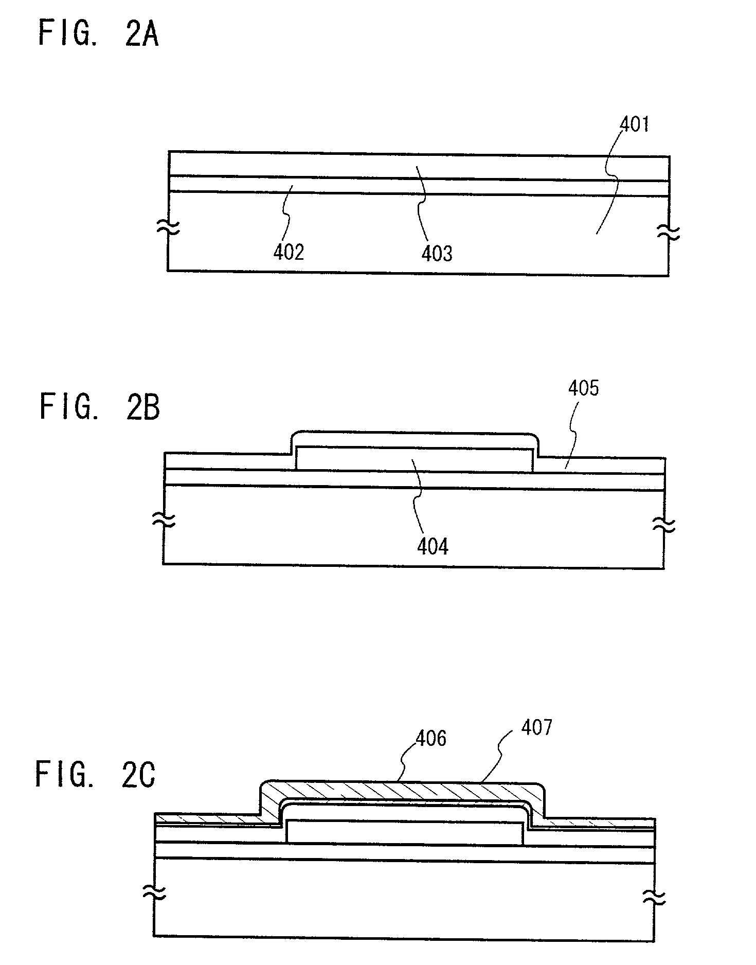
[0069] A detailed explanation will be given by way of the following embodiment. Here, an example, in which a TFT substrate used for a light emitting device is formed.

[0070] In FIG. 2A, a glass substrate or quartz substrate is used for a substrate 401. In the case of using a glass substrate, a substrate film 402 comprising an insulating film is formed on a substrate surface to prevent dispersion of impurities from the substrate.

[0071] Subsequently, a semiconductor layer 403 having a thickness of 25 to 80 nm (preferably, 30 to 60 nm) and an amorphous structure is formed by means of known methods such as the plasma CVD technique and the sputtering method, and a process of crystallization is implemented to fabricate a crystalline semiconductor layer from an amorphous semiconductor layer.

[0072] The laser annealing method and the thermal annealing method (method of crystal growth from solid phase) or the rapid thermal annealing method (RTA method) can be applied as a ...

embodiment 2

[0100] [Embodiment 2]

[0101] An explanation will be given below to a process of fabricating a TFT on a plastic substrate in this embodiment with reference to FIGS. 10A to 10E.

[0102] First, a plastic substrate 201 comprising an organic material is prepared. In this embodiment, the substrate 201 comprising polyimide is used. The substrate comprising polyimide is heat-resistible at about 399.degree. C. and is not transparent but brown-colored. Then a substrate insulating film 202 is formed on the substrate 201. The substrate insulating film is not specifically limitative in a deposition method provided that the method is implemented in a temperature range, in which the plastic substrate is not deformed, preferably a temperature range not exceeding 300.degree. C., and here the sputtering method is used. With the sputtering method, deposition is effected in an atmosphere, in which a sputtering gas does not contain hydrogen, and thus a quantity of hydrogen in the film is 5 atomic % or less...

embodiment 3

[0113] [Embodiment 3]

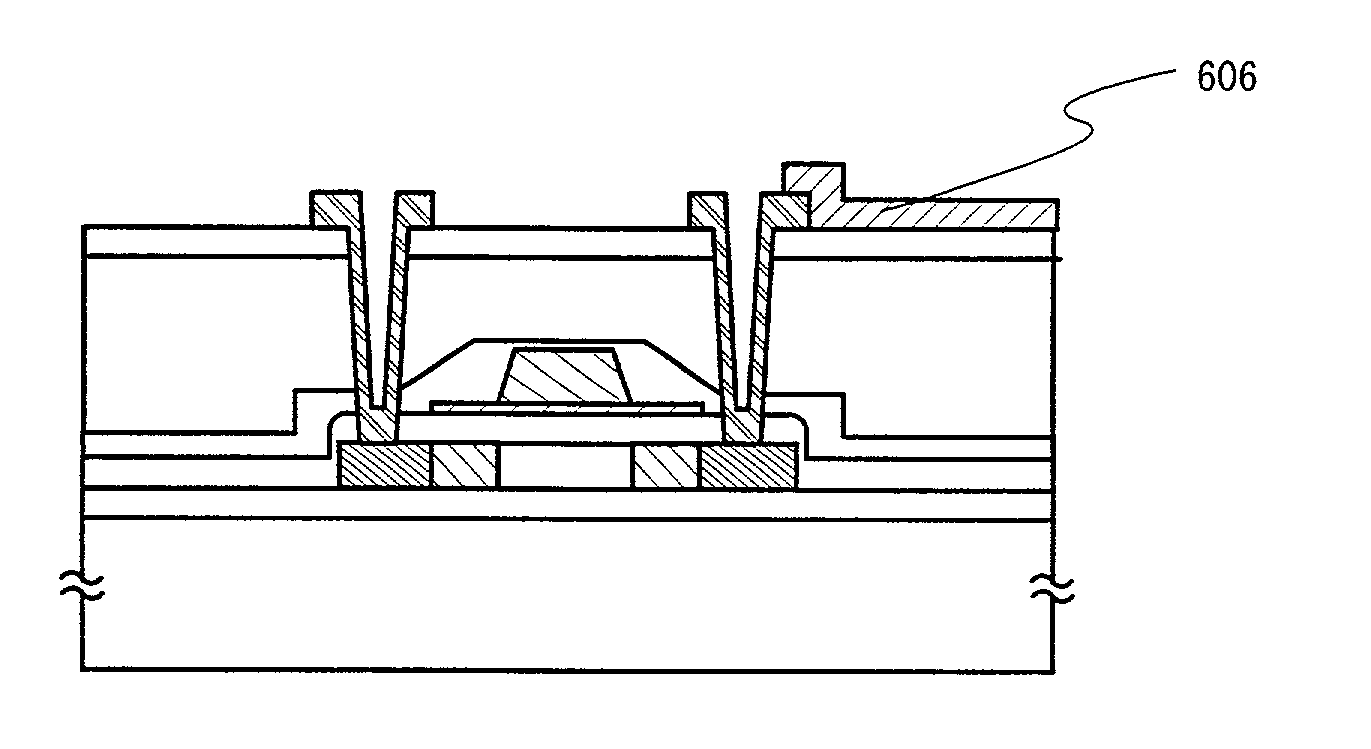
[0114] An example of fabricating an EL (electro-luminescence) display device using the semiconductor device of Embodiment 1 will be explained in this embodiment. Note that FIG. 6A is a top view of an EL display device using the present invention, and FIG. 6B is a cross sectional view thereof.

[0115] In FIG. 6A, reference numeral 4001 denotes a substrate, 4002 denotes a pixel portion, 4003 denotes a source side driving circuit, 4004 denotes a gate side driving circuit. The driving circuits are connected to external equipment, through an FPC (flexible printed circuit) 4006 via a wiring 4005.

[0116] At this time, a first sealing material 4101, a covering material 4102, a filler material 4103 and a second sealing material 4104 are provided so as to enclose the pixel portion 4002, the source side driving circuit 4003, and the gate side driving circuit 4004.

[0117] A cross sectional diagram of FIG. 6 cut along the line A-A' is shown in FIG. 6B. On the substrate 4001, a d...


PUM


Abstract

It is characteristic of an organic material suited to an interlayer insulating film to transmit vapor therethrough and to be liable to absorb moisture, and the material has a disadvantage that it is extremely susceptible to oxygen and moisture to be readily deteriorated no matter whether it is low-molecular or high-molecular. Further, alkali metal or alkaline earth metal is used for a positive electrode or a negative electrode of a light emitting element, and these are liable to be oxidized by oxygen. Thus moisture is responsible for deterioration of a light emitting element and for failure such as dark spots or the like. A light emitting device is provided to comprise an interlayer insulating film comprising a high molecular chemical compound and formed on a TFT formed on an insulating surface, a light emitting element, which is provided on the interlayer insulating film, and in which a light emitting layer comprising an organic chemical compound is formed between a pair of electrodes, and an inorganic insulating film containing silicon and nitrogen as its main components or a carbon film possessing a SP3 coupling and containing hydrogen formed between the interlayer insulating film and the light emitting element.

Description

[0001] 1. Field of the Invention[0002] The invention relates to a light emitting device having, on a substrate with insulating surfaces, a circuit comprising thin film transistors (referred below to as TFT) and a light emitting element between a pair of electrodes to be formed with a light emitting layer.[0003] 2. Related Art[0004] Since TFT can be formed on a transparent substrate, application and development thereof on active matrix type picture display units have been positively promoted Because high mobility can be obtained with TFT, which makes use of a crystalline semiconductor film (typically, crystalline silicon film), picture display of high definition can be realized by integrating function circuits on the same substrate. In recent years, attention has been paid to a technique, in which TFT is constituted by means of a semiconductor thin film (having a thickness in the order of several to several hundreds nm) formed on a substrate having insulating surfaces. TFT has been w...

Claims


Application Information

Patent Timeline
IPC IPC(8): H01L33/00H01L27/32
CPCH01L27/3258H10K59/124H01L23/145H01L2924/13069H01L2924/07025
Inventor TAKAYAMA, TORUYAMAGATA, HIROKAZUKOURA, AKIHIKOYAMAZAKI, SHUNPEI
Owner SEMICON ENERGY LAB CO LTD
Why Eureka
Try Eureka