Optical element fabrication method, optical element, exposure apparatus, device fabrication method

a technology of optical elements and fabrication methods, applied in the direction of lens, crystal growth process, nuclear engineering, etc., can solve the problems of generating optical absorption, deteriorating optical characteristics of optical elements, and damaging the substrate and thin film formed on the substrate, so as to reduce optical absorption and excellent optical characteristics

Inactive Publication Date: 2003-06-12
CANON KK
View PDF6 Cites 16 Cited by
  • Summary
  • Abstract
  • Description
  • Claims
  • Application Information

AI Technical Summary

Benefits of technology

0007] Accordingly, it is an exemplified object of the present invention to provide an optical element fabrication method, exposure apparatus, device fabrication method, and devices, the fabrication method that can reduce an optical absorption produced when a thin film is fabricated on a substrate and can fabricate an optical element having excellent optical characteristics. The present invention is especially effective when the substrate includes fluoride crystal(s).

Problems solved by technology

However, the shorter the wavelength becomes, the larger light's absorption, diffusion, and interference become, and thus, along with a shorter wavelength of light from a light source, the reflection of light on the surface of an optical element such as a lens and a mirror cannot be neglected.
However, if a thin film is formed onto a substrate by using the sputtering and CVD methods that use plasma, and by the vacuum evaporation method that uses an electron gun, an electric potential difference is produced among ion, electron and the substrate, and the ion and electron breaks into the substrate, thus damaging the substrate and the thin film formed on the substrate.
This damage would change a compositional ratio of chemical compounds, and impair crystallization, thereby deteriorating optical characteristics of an optical element.
This damage includes generation of optical absorption (the so-called color center that absorbs light).
Then, although it is electrically stable, it is hard for light to transmit it, thus reducing its transmittance.
In particular, optical absorption is noticeably observed in a light wavelength range equal to or shorter than 300 nm, thus presenting the problem that a transmission type optical element reduces its transmittance, being unable to obtain expected optical characteristics.

Method used


Image

  • Optical element fabrication method, optical element, exposure apparatus, device fabrication method
  • Optical element fabrication method, optical element, exposure apparatus, device fabrication method
  • Optical element fabrication method, optical element, exposure apparatus, device fabrication method

Examples


example 2

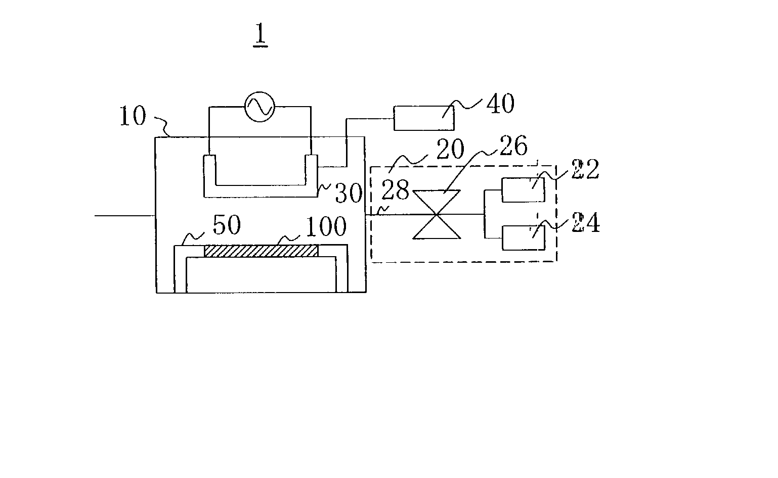
[0038] At first, a thin film of magnesium fluoride ("MgF.sub.2") with a thickness of about 100 nm was formed by vaporizing the magnesium fluoride while heating it with an electron beam, onto a flat CaF.sub.2 substrate with a thickness of 2 mm, both of whose surfaces are polished to be used as the substrate 100. As soon as the thin film was formed, the transmittance and reflectance of this optical element was measured using a spectrophotometer to calculate an optical absorption factor.

[0039] Next, this optical element was irradiated by a low-pressure mercury lamp for one hour (where it is assumed that the irradiating section 30 of the optical irradiation apparatus 1 is a low-pressure mercury lamp). After this optical element was irradiated by the low-pressure mercury lamp, its transmittance and reflectance was measured again by using the spectrophotometer to calculate its optical absorption factor.

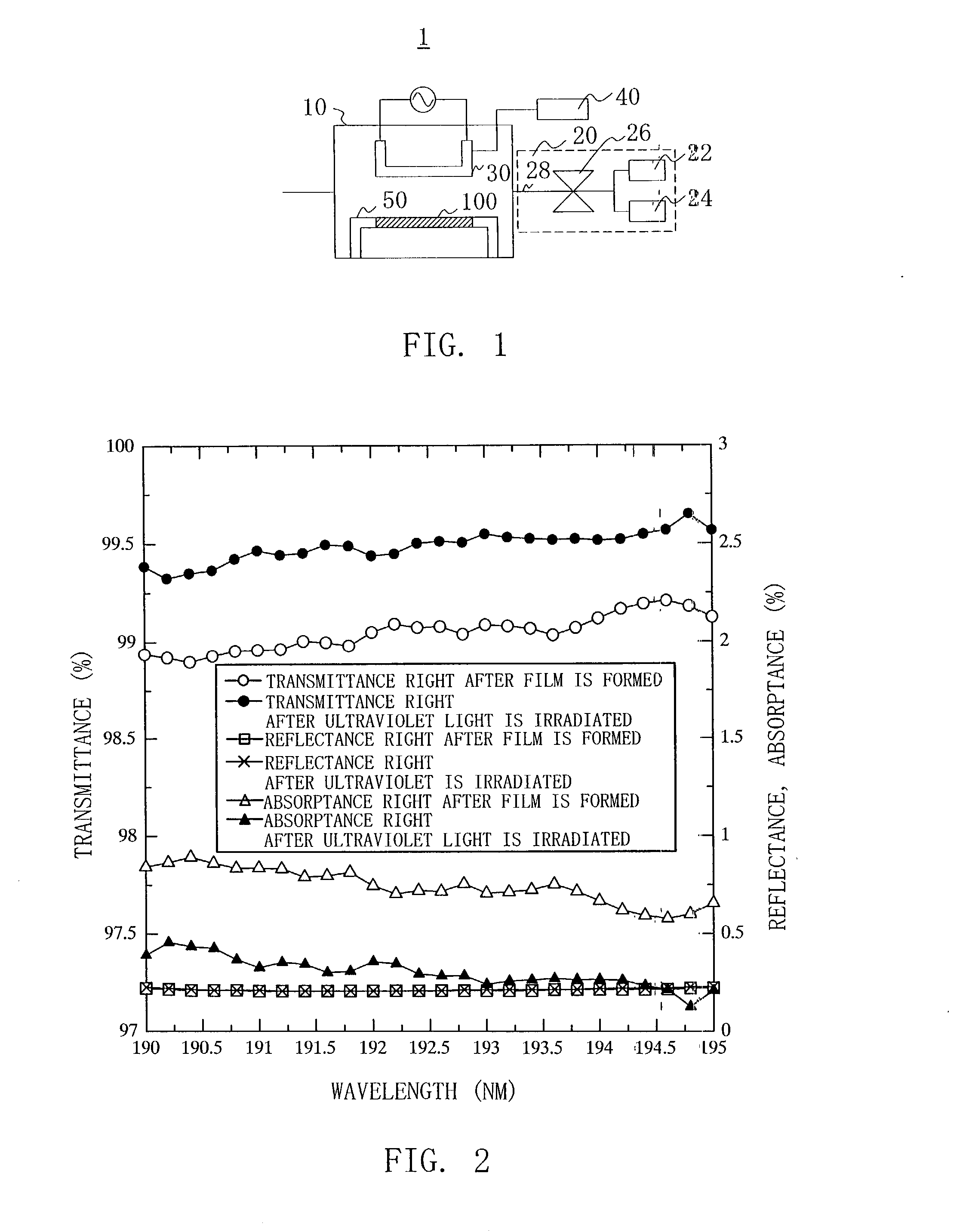
[0040] The calculation result of the optical absorption factor at the wavelength of 248...

example 3

[0041] Similar to the second embodiment, a thin film of MgF.sub.2 with a thickness of about 100 nm was first formed by vaporizing the MgF.sub.2 while heating it with an electron beam, onto a flat CaF.sub.2 substrate with a thickness of 2 mm, both of whose surfaces are polished to be used as the substrate 100. As soon as the thin film was formed, the transmittance and reflectance of this optical element was measured using a spectrophotometer to calculate its optical absorption factor.

[0042] Next, this optical element was irradiated by KrF excimer laser for 30 minutes (where it is assumed that the irradiating section 30 of the optical irradiation apparatus 1 is KrF excimer laser). After this optical element was irradiated by the KrF excimer laser, its transmittance and reflectance was measured again by using the spectrophotometer to calculate its optical absorption factor.

[0043] The calculation result of the optical absorption factor at the wavelength of 248 nm from the measured trans...

example 4

[0044] Similar to embodiment 1, an alumina thin film with a thickness of about 100 nm was first formed by the sputtering method onto a flat MgF.sub.2 substrate with a thickness of 2 mm, both of whose surfaces are polished to be used as the substrate 100. As soon as the thin film was formed, the transmittance and reflectance of this optical element was measured using a spectrophotometer to calculate its optical absorption factor.

[0045] Next, this optical element was irradiated by ArF excimer laser for one hour (where it is assumed that the irradiating section 30 of the optical irradiation apparatus 1 is ArF excimer laser). After this optical element was irradiated by ArF excimer laser, its transmittance and reflectance was measured again by using the spectrophotometer to calculate its optical absorption factor.

[0046] The calculation result of the optical absorption factor at the wavelength of 193 nm from the measured transmittance and reflectance was 1.5% right after the thin film wa...


PUM

PropertyMeasurementUnit
wavelength rangeaaaaaaaaaa
wavelengthaaaaaaaaaa

Abstract

There is to provide an optical element fabrication method including the steps of forming a thin film onto a substrate, and eliminating a color center produced in the forming step by giving energy to the substrate.

Description

[0001] The present invention generally relates to optical element fabrication methods, and more particularly to a fabrication method for a transmission type optical element including a thin film. The present invention is suitably applicable for fabricating fluoride crystal materials such as calcium fluoride, magnesium fluoride, etc. suitable for various kinds of optical elements, lenses, window materials, prisms, etc. employed in a wide wavelength range, e.g., from the vacuum ultraviolet region to the far-infrared region.[0002] Fluoride crystal has distinguished characteristics, which other optical materials do not have, such as less dispersion for white light, high transmittance for light having a wavelength shorter than the ultraviolet region, etc., thus having been so far used for a telescope lens with high resolution and low aberration. Recently, applications to a lens in an illumination optical system and a projection optical system in an exposure apparatus have been reviewed w...

Claims


Application Information

Patent Timeline
Patent Type & Authority Applications(United States)
IPC IPC(8): G02B5/18C03C17/00C03C23/00C23C14/58C30B33/00G02B1/10G02B1/11G02B1/113G02B3/00G03F7/20
CPCC03C17/001C03C23/0005C03C2218/32C30B33/00G03F7/70958C30B29/12
Inventor BIRO, RYUJIOTANI, MINORU
Owner CANON KK
Why Eureka
Try Eureka