Resist pattern thickening material, resist pattern and forming process thereof, and semiconductor device and manufacturing process thereof

a resist pattern and thickening material technology, applied in the direction of photosensitive material processing, photomechanical equipment, instruments, etc., can solve the problems of insufficient resist pattern used for exposure, insufficient resist pattern for etching resistance, and large expens

Inactive Publication Date: 2003-08-21
FUJITSU LTD
View PDF9 Cites 56 Cited by
  • Summary
  • Abstract
  • Description
  • Claims
  • Application Information

AI Technical Summary

Benefits of technology

[0013] The present invention has a further object to provide a resist pattern which can be patterned by using ArF excimer laser, has a fine structure, and is excellent in etching resistance.
[0014] Another object of the present invention is to provide a process for forming a resist pattern capable of using ArF excimer laser light as exposure light with excellent mass-productivity and forming a fine pattern by the resist pattern over the exposure limit of light with low cost, with ease, and with improving etching resistance.

Problems solved by technology

However, in order to shorten the wavelength of the optical source at the exposure device, it is indispensable to renew an exposure device, which results in considerable expenses.
Developing a resist material which suits an exposure with a shorter wavelength is not very easy.
However, the newest technique, an ArF (argon fluoride) excimer laser exposure, has a problem that a resist pattern used for the exposure is insufficient in etching resistance.
It is possible to use a KrF (krypton fluoride) resist, but the KrF resist sometimes has insufficient etching resistance in a case of a severe etching condition, a thick treating layer, forming a fine pattern, and having a thin resist thickness.

Method used


Image

  • Resist pattern thickening material, resist pattern and forming process thereof, and semiconductor device and manufacturing process thereof
  • Resist pattern thickening material, resist pattern and forming process thereof, and semiconductor device and manufacturing process thereof
  • Resist pattern thickening material, resist pattern and forming process thereof, and semiconductor device and manufacturing process thereof

Examples


example 1

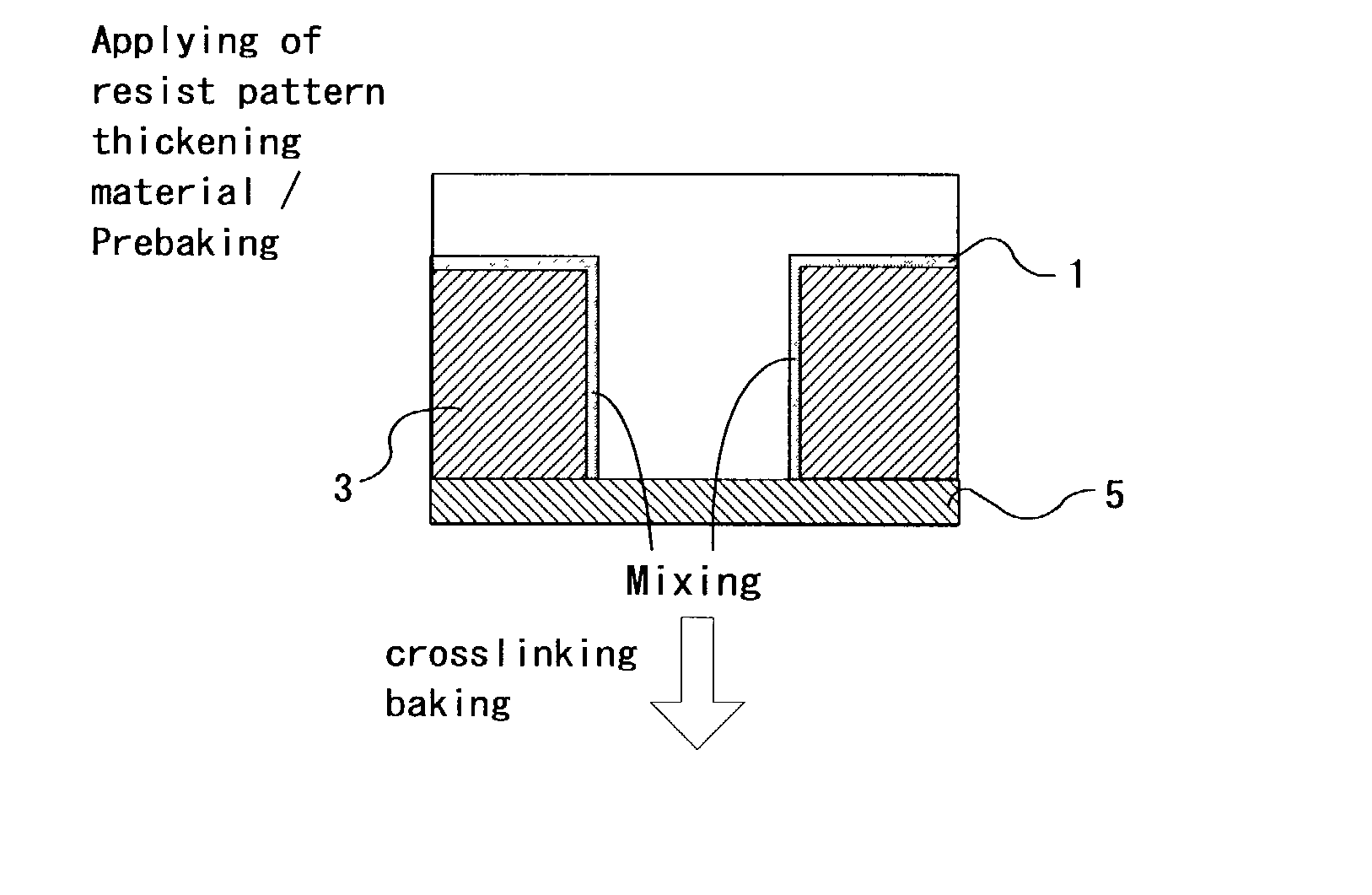
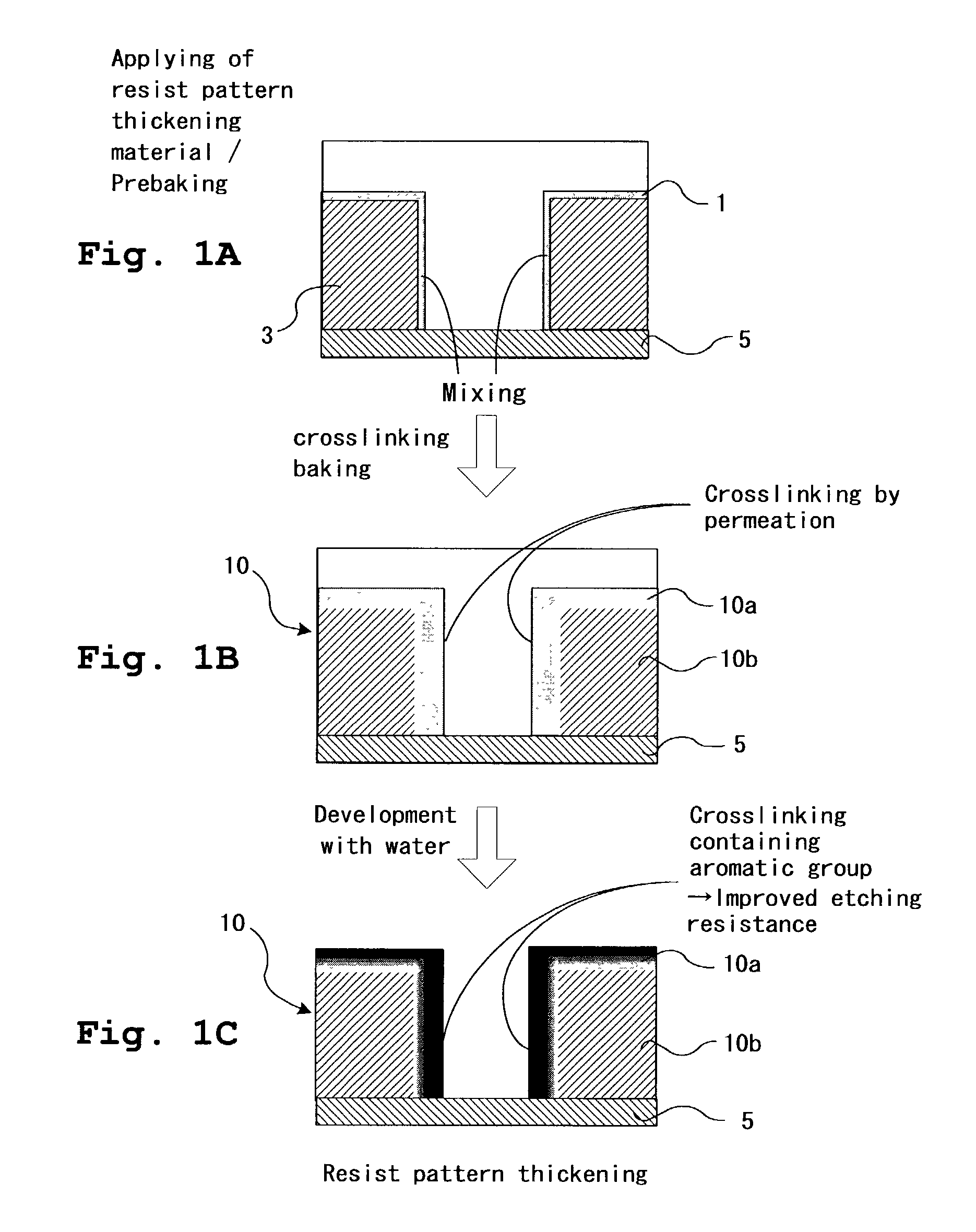
[0178] Preparation of Resist Pattern Thickening Material

[0179] Resist pattern thickening materials 1A-1J according to the present invention having compositions shown in Table 1 were prepared. In Table 1, the unit of the numeric in parentheses represents a part by mass. In the column of "Resin", "KW3" represents a polyvinyl acetal resin (manufactured by SEKISUI CHEMICAL Co., Ltd.), and "PVA" shows a polyvinyl alcohol resin (manufactured by KURARAY Co., Ltd, Poval 117). In the column of "Crosslinking agent", "Uril" represents tetramethoxymethyl glycoluril, "Urea" represents N,N'-dimethoxymethyl dimethoxyethyleneurea, and "Melamine" represents hexamethoxymethylmelamine. In the column of "Surfactant", "TN-80" represents a non-ionic surfactant (manufactured by ASAHI DENKA Co., Ltd., a primary alcohol ethoxylate type surfactant), "PC-6" represents a non-ionic surfactant (ASAHI DENKA Co., Ltd., a special phenol ethoxylate type surfactant), "PC-8" represents a non-ionic surfactant (ASAHI DE...

example 2

[0190] Preparation of Resist Pattern Thickening Material

[0191] Resist pattern thickening materials 2A-2M according to the present invention having compositions shown in Table 5 were prepared. In Table 5, the unit of the numeric in parentheses represents a part by mass. In the column of "Resin", "Resin 1", "Resin 2" and "Resin 3" are synthesized as shown hereinafter. In the column of "Crosslinking agent," "Uril" represents tetramethoxymethyl glycoluril, "Urea" represents N,N'-dimethoxymethyl dimethoxyethyleneurea, and "Melamine" represents hexamethoxymethylmelamine. In the column of "Surfactant", "TN-80" represents a non-ionic surfactant (manufactured by ASAHI DENKA Co., Ltd., a primary alcohol ethoxylate type surfactant). As the main solvent component except the above resins, crosslinking agents, and surfactant agents and a mixture of pure water (deionized water) and isopropyl alcohol (mass ratio of pure water (deionized water) to isopropyl alcohol=16:0.75) was used. "Resin 1" is a ...

example 3

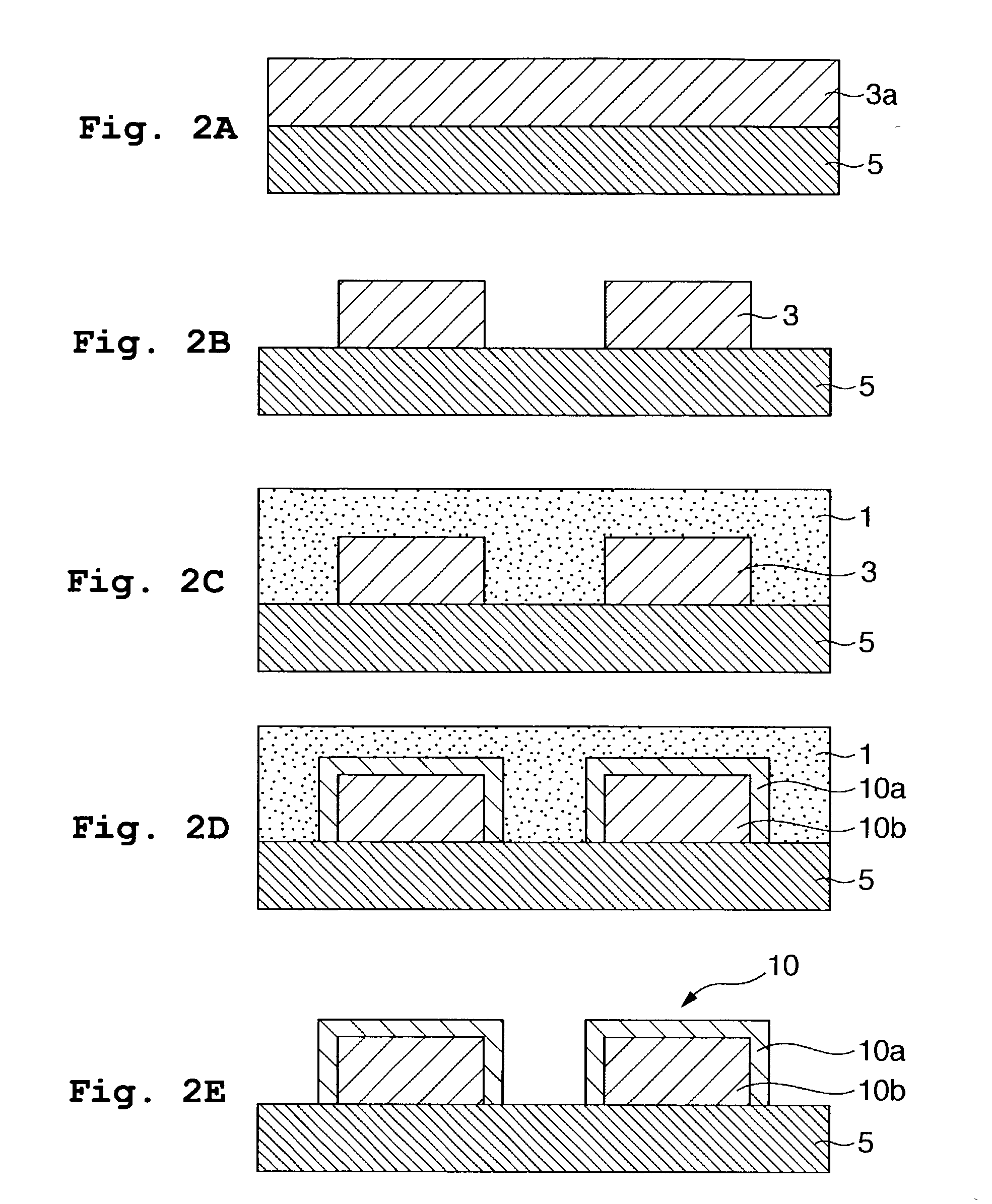
[0205] Flash Memory and its Manufacture

[0206] Example 3 is one embodiment of the semiconductor device and manufacturing process thereof of the present invention using the resist pattern thickening material of the present invention. In Example 3, resist films 26, 27, 29, 32 and 34 are thickened by use of the resist pattern thickening material of the present invention according to the same process as in Examples 1 and 2.

[0207] FIGS. 3A and 3B are upper surface views (plan views) of a FLASH EPROM called FLOTOX type or ETOX type. FIGS. 4A to 4C, FIGS. 5D to 5F, and FIGS. 6G to 6I are schematic sectional views for showing one example for the manufacturing process for the FLASH EPROM, wherein the left views in FIGS. 4A through 6I are schematic sectional (A-directional sectional) views in the gate lateral direction (X-direction in FIGS. 3A and 3B) of the part for forming a MOS transistor having a floating gate electrode in a memory cell pat (first element region), the central views are sch...


PUM

PropertyMeasurementUnit
wavelengthaaaaaaaaaa
boiling pointaaaaaaaaaa
thicknessaaaaaaaaaa

Abstract

A resist pattern thickening material has resin, a crosslinking agent and a compound having a cyclic structure, or resin having a cyclic structure at a part. A resist pattern has a surface layer on a resist pattern to be thickened with etching rate (nm / s) ratio of the resist pattern to be thickened the surface layer of 1.1 or more, under the same condition, or a surface layer to a resist pattern to be thickened. A process for forming a resist pattern includes applying the thickening material after forming a resist pattern to be thickened on its surface. A semiconductor device has a pattern formed by the resist pattern. A process for manufacturing the semiconductor device has applying, after forming a resist pattern to be thickened, the thickening material to the surface of the resist pattern to be thickened, and patterning the underlying layer by etching, the pattern as a mask.

Description

[0001] This application is based upon and claims the benefit of priority from the prior Japanese Patent Application No. 2001-361505, filed on Nov. 27, 2001, the prior Japanese Patent Application No. 2002-139317, filed on May 14, 2002 and the prior Japanese Patent Application No. 2002-328931, filed on Nov. 12, 2002, the entire contents of which are incorporated herein by reference.[0002] 1. Field of the Invention[0003] The present invention relates to a resist pattern thickening material which thickens a resist pattern by being applied onto a resist pattern that is formed of an ArF resist, may form a fine pattern exceeding exposure limit of optical source of an exposure device, and allows for improving etching resistance of the resist pattern; a resist pattern which may be patterned by an ArF excimer laser and the like, has a fine structure, and is excellent in etching resistance; and an efficient process for forming the resist pattern; a semiconductor device having a fine pattern fo...

Claims


Application Information

Patent Timeline
Patent Type & Authority Applications(United States)
IPC IPC(8): G03F7/00G03F7/40G11B5/17G11B5/31H01L21/027H01L21/8247H01L27/115
CPCG03F7/0035G03F7/40G11B5/17G11B5/312G11B5/3163H01L27/11543H01L21/0273H01L21/32139H01L27/105H01L27/115H01L27/11526H01L21/0271H10B41/48H10B41/40H10B69/00
Inventor KOZAWA, MIWANOZAKI, KOJINAMIKI, TAKAHISAKON, JUNICHIYANO, EI
Owner FUJITSU LTD
Why Eureka
Try Eureka