

Field electron emission apparatus and method for manufacturing the same
- Summary
- Abstract
- Description
- Claims
- Application Information
AI Technical Summary
Benefits of technology
Problems solved by technology
Method used
Image

Examples
example 2
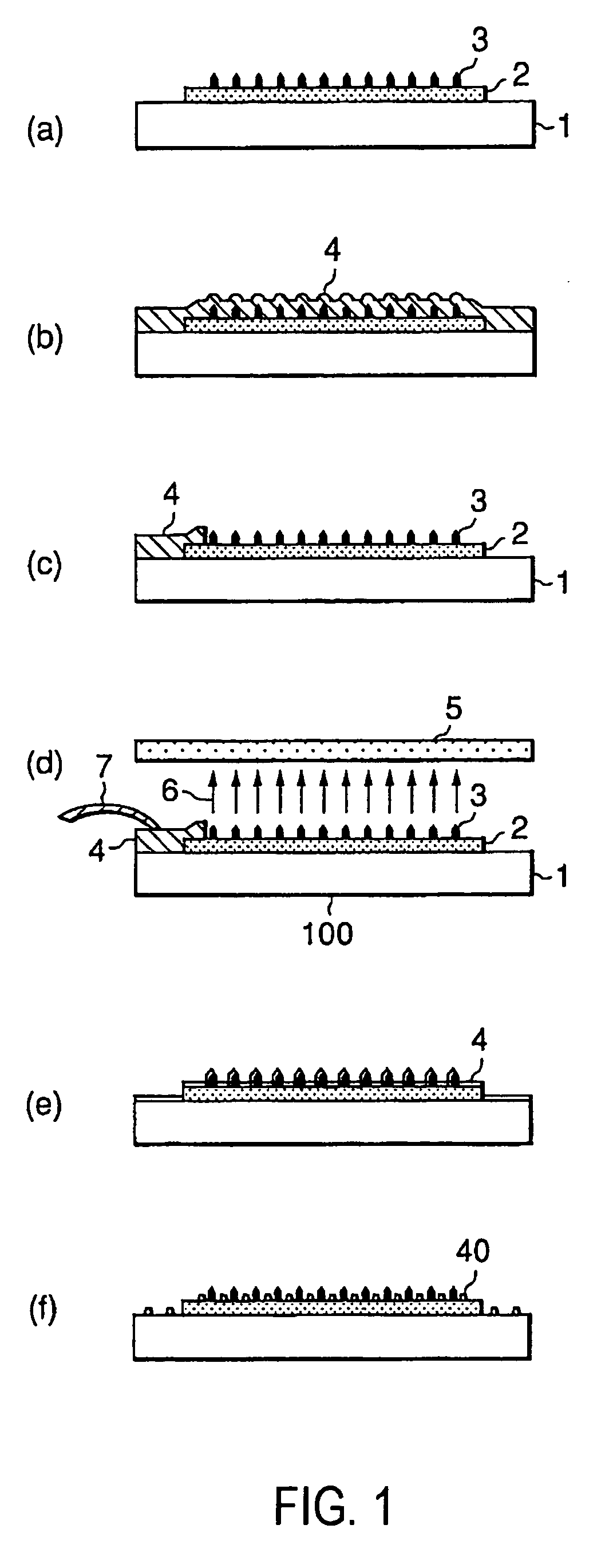
[0060] FIGS. 1(e) and (f) are sectional side views showing stages in a manufacturing process for a field electron emission apparatus. This process is a specific example of a method for manufacturing a field electron emission apparatus according to Example 2 of the present invention. The stages shown in FIGS. 1(e) and (f) are individually substitutes for the condition of the second step shown in FIG. 1(b) through the condition of the fourth steps shown in FIG. 1(d), and in the stages, the fine structure 3 is in the condition of being covered with an aluminum film.
[0061] The condition of the fourth step shown in FIG. 1(e) indicates a condition in which the aluminum film 4 having a film thickness of 10 nm is adhered to the fine structure 3. Here, the aluminum film 4 protects the fine structure 3 from a reaction during the process, and in addition, the fine structure 3 is covered with the aluminum film 4. Consequently, the aluminum film 4 becomes a part of the fine structure 3, and the ...
example 3
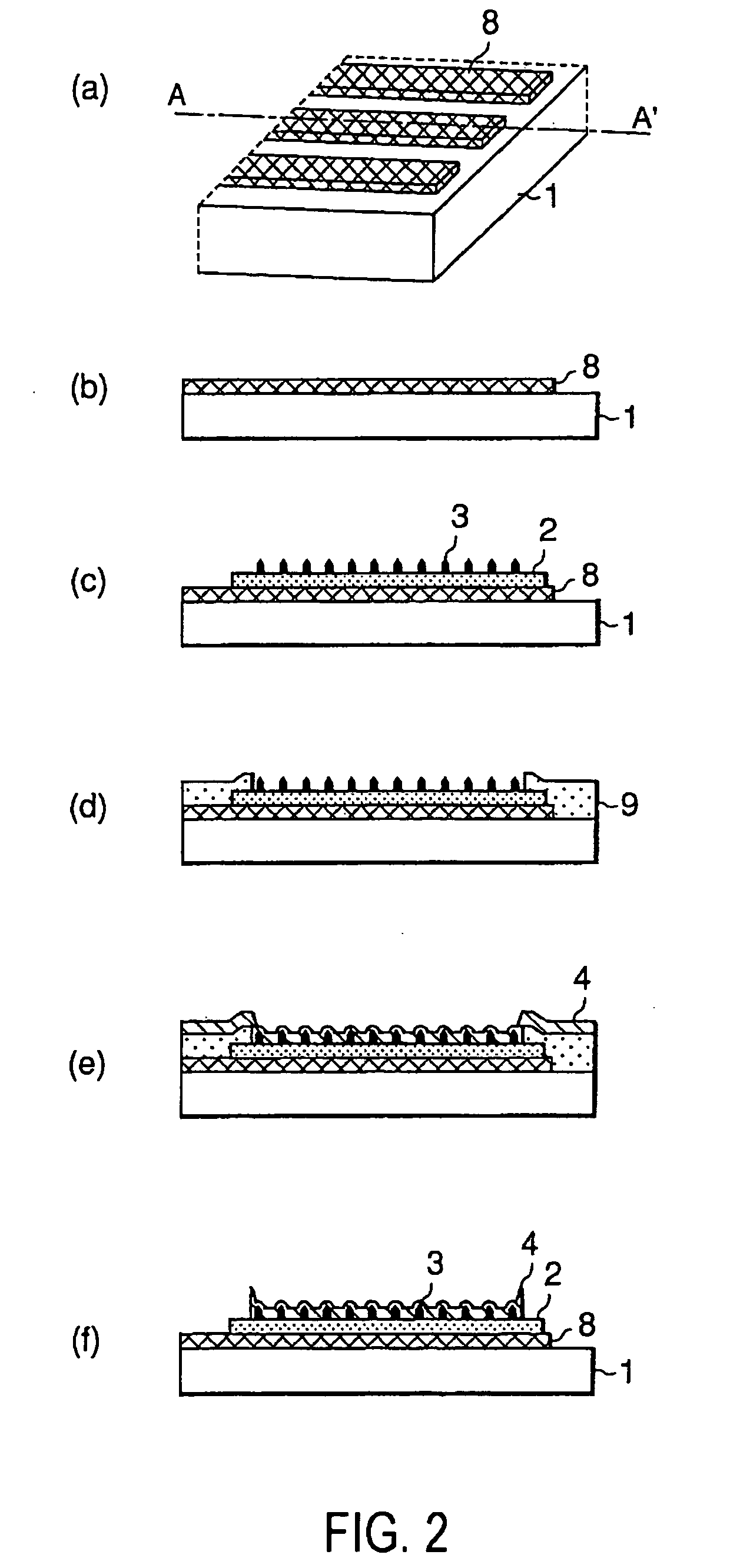
[0063] FIGS. 2(a) to (f) are sectional side views showing a manufacturing process for a field electron emission apparatus in a step-by-step manner. The process is a specific example of a method for manufacturing a field electron emission apparatus according to Example 3 of the present invention, and in this process, a cathode wiring is arranged on a glass substrate, and thereafter, a CNT film is deposited.
[0064] As the first step, cathode wirings 8 are patterned on a glass substrate 1 into a stripe-like shape. The resulting pattern of the cathode wirings 8 is shown in a partial perspective view shown in FIG. 2(a), and in a sectional side view shown in FIG. 2(b) in the direction A-A' indicated in FIG. 2(a).
[0065] As the second step, a CNT film 2 is formed on the cathode wiring 8. In the resulting condition, a fine structure 3 is arranged on the surface of the CNT film 2, as shown in FIG. 2(c). Here, the CNT film 2 is formed on each of the wirings of the cathode wirings 8 on the strip...
example 4
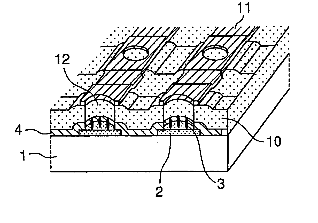
[0070] FIGS. 3(a) to (d) are sectional side views showing a manufacturing process for a triode-structure field electron emission apparatus in a step-by-step manner, and this apparatus has a gate conductive film. The process is a specific example of a method for manufacturing a field electron emission apparatus according to Example 4 of the present invention. Here, the fine structure 3 is an electron emission source, and is assumed to be the cathode electrode. In addition, a structure referred to as a triode structure includes three electrodes composed of a cathode electrode, a gate electrode and an electron capture electrode (a phosphor screen and a metal anode electrode). In this triode structure, the amount of emitted electrons can be controlled by adjusting a potential difference between the gate electrode and the cathode electrode.
[0071] Since the first step shown in FIG. 3(a) is the same as the condition shown in FIG. 2(f), explanations thereof are omitted.
[0072] In the second ...
PUM
 Abstract
Description
Claims
Application Information