
Method of generating ballistic electrons and ballistic electron solid semiconductor element and light emitting element and display device

a technology of applied in the field of generating ballistic electrons and ballistic electron solid semiconductor elements and light emitting elements and display devices, can solve the problems of no research or development obtaining excellent, decrease of device thickness or increase of device size,

Inactive Publication Date: 2004-05-06
JAPAN SCI & TECH CORP
View PDF1 Cites 5 Cited by
  • Summary
  • Abstract
  • Description
  • Claims
  • Application Information

AI Technical Summary

Benefits of technology

[0036] In a ballistic conduction mode, electrons travel in a solid without being scattered. That is, because heat due to electron conduction is not produced, it is possible to realize a state like a vacuum tube in which the operation space and heat-radiation space of a device are separated from each other though the device is solid. Moreover, in the case of a normal semiconductor, after an electron velocity reaches a saturated drift velocity decided by the balance between electron acceleration and photon scattering, it is impossible to accelerate electrons further even if increasing an electric field. Therefore, the operation frequency of a semiconductor device is limited. However, the saturated drift velocity of a ballistic electron is not limited. Therefore, by applying a ballistic-electron solid-state semiconductor device of the invention of the present application, it is possible to realize an electron device to be driven at an ultra-high speed and having an extremely low energy loss.
[0042] Moreover, by functionally integrating a ballistic-electron solid-state semiconductor device of the invention of the present application with a VLSI, it is possible to realize a video-information display device or an arithmetic processing unit.

Problems solved by technology

However, most of the studies remain at physical observation under a very restricted condition such as a specific single structure or very low temperature and thus, they have not resulted in the industrial device development.
However, it is the present state that there is almost no research or development obtaining excellent results from the above viewpoint.
Therefore, this has been a large fault against decrease of a device in thickness or increase of the device in size.
Therefore, the emission quantum efficiency is restricted to a limited value by an energy loss in the photon conversion of carriers in the solid and therefore, heat generation in the element is unavoidable.
Therefore, to increase a display device in size, actions for deterioration of device characteristics due to a temperature rise and for thermal sinking are left as technical problems.
Also concerning a plasma display, restriction of emission due to energy loss under operation is a problem and moreover, the fact that it is difficult to realize small-power driving because of using discharge is left as a problem to be solved.
Thus, a natural-light display device has advantages and disadvantages depending on its type and has many technical subjects such as increase in size, decrease in thickness, and decrease in power consumption.

Method used


Image

  • Method of generating ballistic electrons and ballistic electron solid semiconductor element and light emitting element and display device
  • Method of generating ballistic electrons and ballistic electron solid semiconductor element and light emitting element and display device
  • Method of generating ballistic electrons and ballistic electron solid semiconductor element and light emitting element and display device

Examples


example 1

[0045] A ballistic-electron-exciting solid-state light-emitting device of the invention of the present application is fabricated and basic characteristics are studied.

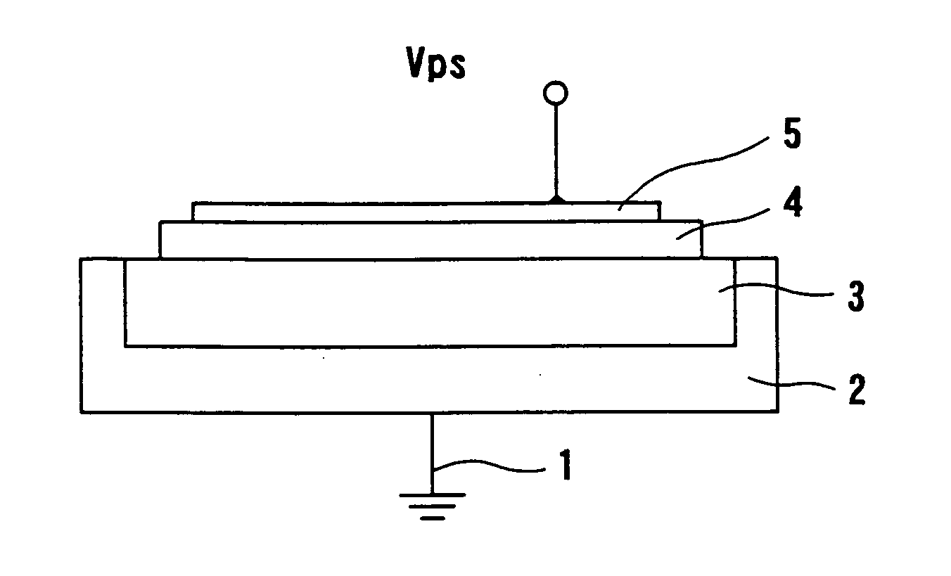
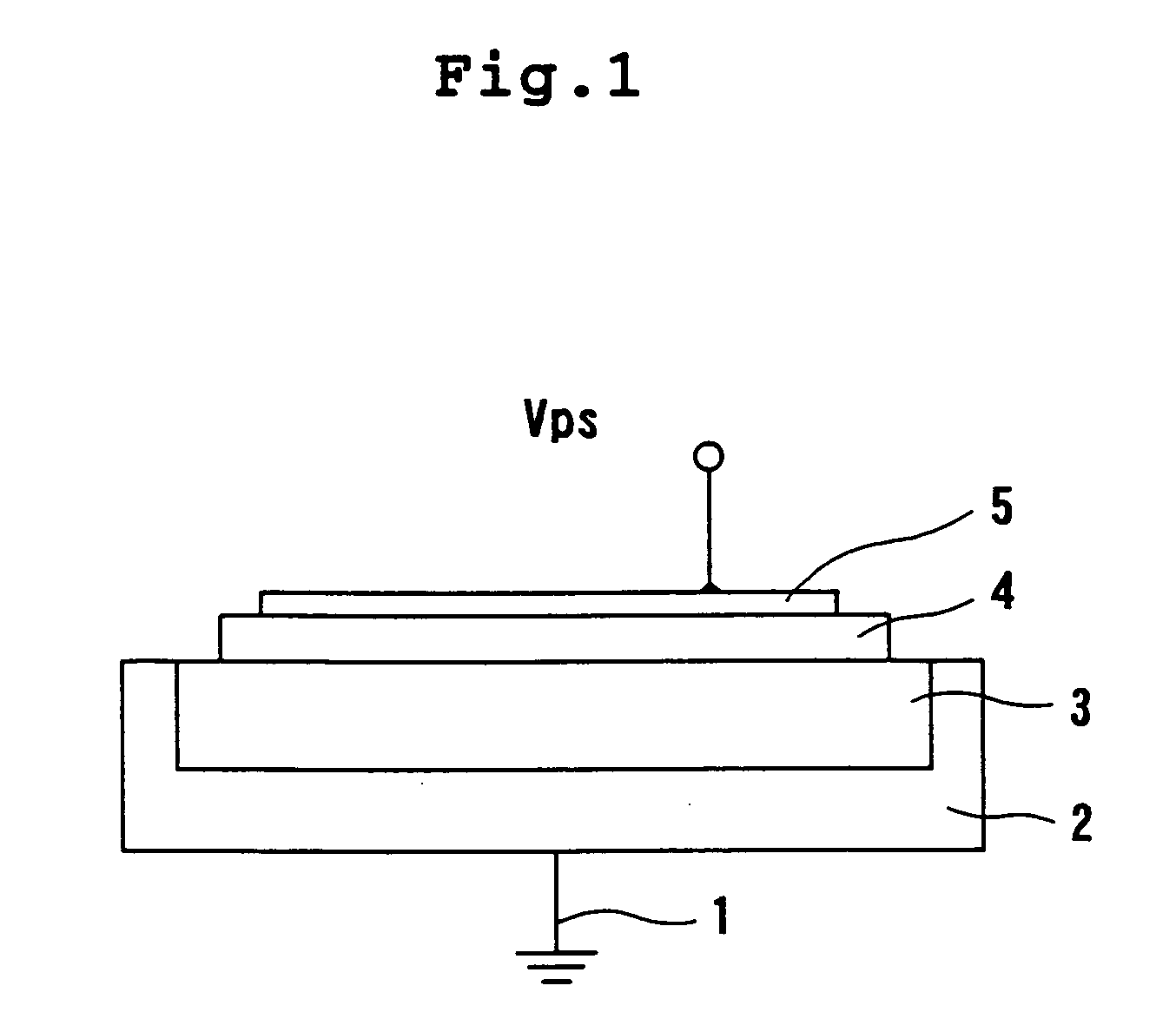
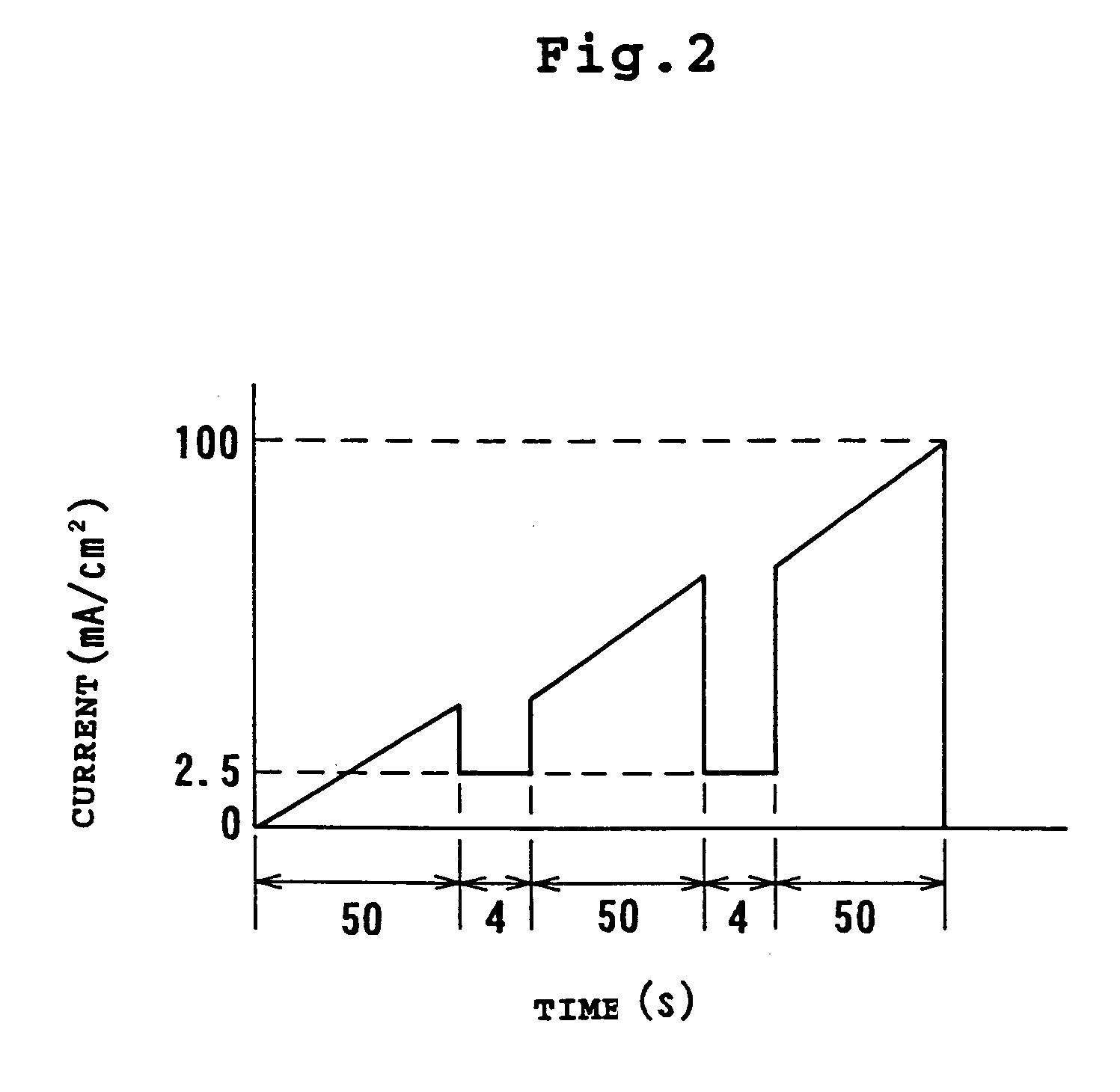
[0046] As shown in FIG. 1, in the case of a fabricated ballistic-electron-exciting solid-state semiconductor device, a PS layer (3) is formed by applying anodic oxidation to the surface of an n-type silicon substrate (2) (resistivity of 0.018 .OMEGA.cm) having a orientation (111) on whose back an ohmic electrode (1) is formed in a mixed solution (mixture rate of 1:1) of 50 wt % HF aqueous solution and ethanol under light irradiation using a 500-W tungsten lamp as a light source. In this case, as shown in FIG. 2, the operation of slowly increasing an anodic oxidation current for 158 sec and decreasing the anodic oxidation current up to 2.5 mA / cm.sup.2 every 4 sec in the middle of the above period of 158 sec is performed twice. Finally, the anodic oxidation current becomes 100 mA / cm.sup.2.

[0047] The PS layer (3) has a th...

example 2

[0055] Another ballistic-electron-exciting solid-state light-emitting device of the invention of the present application is fabricated to study the basic characteristic.

[0056] The example 2 uses the n-type silicon substrate (2) constituted as shown in FIG. 1 as a p-type silicon substrate. Specifically, a PS layer (3) is formed by applying anodic oxidation to the surface of a p-type silicon substrate (resistivity: approx. 0.2 .OMEGA.cm) which has an orientation (100) and on whose back an ohmic electrode (1) is formed in a solution obtained by mixing an HF aqueous solution (55 wt %) and C.sub.2H.sub.5OH at a ratio of 1:1 under a darkroom state and moreover applying quick thermal oxidation at 900.degree. C. for 15 min. In the case of the anodic oxidation, a cycle of an anodic oxidation current of 5 mA / cm.sup.2 and an anodic oxidation time of 6 sec and a cycle of an anodic oxidation current of 100 mA / cm.sup.2 and an anodic oxidation time of 15 sec are alternately repeated three times.

[0...

example 3

[0059] Still another ballistic-electron-exciting solid-state light-emitting device of the invention of the present application is fabricated to study the basic characteristic.

[0060] The example 3 uses the PS layer (3) constituted as shown in FIG. 1 as a nano-cyrstallized polysilicon film. Specifically, an n.sup.+-type polysilicon film (thickness of 5 .mu.m) is first formed on the surface of an n-type silicon substrate (resistivity: 0.005 to 0.0018 .OMEGA.cm) which has an orientation (100) and on whose back an ohmic electrode (1) is formed. Then, a porous polysilicon (PPS) film is formed by applying anodic oxidation up to almost the half depth of the n.sup.+-type polysilicon film in a solution obtained by mixing an HF aqueous solution (55 wt %) and C.sub.2H.sub.5OH at a ratio of 1:1 under irradiation by a tungsten lamp and moreover applying electrochemical oxidation to the silicon film in a 1NH.sub.2SO.sub.4 solution under a darkroom state. In the case of the anodic oxidation, a cycl...


PUM


Abstract

A method of generating ballistic electrons with a high controllability by applying an electric field to a nano-structure micro-crystal layer or a semi-insulating layer of a semiconductor to generate ballistic electrons or quasiballistic electrons by a multiple-tunnel effect; and a semiconductor device used in this method and provided with a practical material constitution.

Description

[0001] The present invention relates to a ballistic-electron solid-state semiconductor device. More particularly, the present invention relates to a ballistic-electron solid-state semiconductor device for realizing ballistic conduction in which the drift length in a semiconductor extremely increases under a high electric field and using generated ballistic electrons as an excitation source.[0002] It is known that electrons travel without being scattered and behave like electrons in a vacuum by decreasing the size of a semiconductor up to a dimensional region smaller than the mean free path of electrons in the semiconductor. The conduction electrons are referred to as ballistic electrons that can travel without being scattered or with no loss even in a solid differently from normal conduction electrons based on drift or diffusion.[0003] Because it is estimated that the semiconductor device technology is greatly innovated when ballistic electrons can be obtained at a high controllabil...

Claims


Application Information

Patent Timeline
IPC IPC(8): H01J1/308H01J1/312H01J31/12H01J63/06
CPCB82Y10/00H01J63/06H01J31/127H01J1/312H01L29/66
Inventor KOSHIDA, NOBUYOSHI
Owner JAPAN SCI & TECH CORP
Learn More